System Overview
3-10
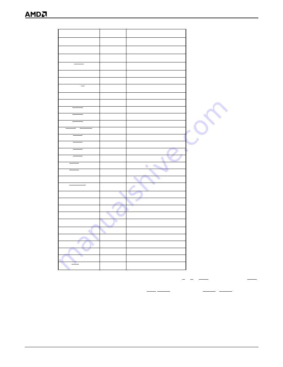
Table 3-2
PIO Pin Assignments—Alphabetic Listing
Notes:
1. These pins are used by emulators. (Emulators also use
S2–S0
,
RES
, NMI, CLKOUTA,
BHE
,
ALE, AD15–AD0, and A16–A0.
2. These pins revert to normal operation if
BHE/ADEN
(Am186EM) or
RFSH2/ADEN
(Am188EM)
is held Low during power-on reset.
3. When used as a PIO, input with pullup option available.
4. When used as a PIO, input with pulldown option available.
Associated Pin
PIO No.
Power-On Reset Status
A17
(1)
7
Normal operation
(3)
A18
(1)
8
Normal operation
(3)
A19
(1)
9
Normal operation
(3)
DEN
5
Normal operation
(3)
DRQ0
12
Input with pullup
DRQ1
13
Input with pullup
DT/R
4
Normal operation
(3)
INT2
31
Input with pullup
INT4
30
Input with pullup
MCS0
14
Input with pullup
MCS1
15
Input with pullup
MCS2
24
Input with pullup
MCS3/RFSH
25
Input with pullup
PCS0
16
Input with pullup
PCS1
17
Input with pullup
PCS2
18
Input with pullup
PCS3
19
Input with pullup
PCS5/A1
3
Input with pullup
PCS6/A2
2
Input with pullup
RXD
28
Input with pullup
S6/CLKDIV2
(1,2)
29
Input with pullup
SCLK
20
Input with pullup
SDATA
21
Input with pullup
SDEN0
22
Input with pulldown
SDEN1
23
Input with pulldown
SRDY
6
Normal operation
(4)
TMRIN0
11
Input with pullup
TMRIN1
0
Input with pullup
TMROUT0
10
Input with pulldown
TMROUT1
1
Input with pulldown
TXD
27
Input with pullup
UZI
(1,2)
26
Input with pullup
Содержание AM186EM
Страница 1: ...Am186 EM and Am188 EM Microcontrollers User s Manual...
Страница 4: ...iv...
Страница 12: ...Table of Contents xii...
Страница 62: ...Peripheral Control Block 4 10...
Страница 76: ...Chip Select Unit 5 14...
Страница 122: ...Timer Control Unit 8 8...
Страница 136: ...DMA Controller 9 14...
Страница 144: ...Asynchronous Serial Port 10 8...
Страница 158: ...Programmable I O Pins 12 6...
Страница 186: ...Index I 12...