ADM-SDEV-BASE/XCKU060 User Manual
V1.0 - 27th November 2018
3.6 FPGA
3.6.1 I/O Bank Voltages
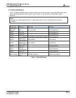
The FPGA IO is arranged in banks, each with their own supply pins. The bank numbers, their voltage and
function are shown in
Target FPGA IO Banks
. Full details of the IOSTANDARD required for each signal are
given in the ADA-SDEV-BASE SDK.
IO Banks
Voltage
Purpose
0, 65
FMC2_VIO_B
Configuration, JTAG
44, 45
FMC1_VADJ
LPC FMC GPIO
24, 64
FMC2_VADJ
Config FMC GPIO
25, 46, 47
FMC3_VADJ
FMC+ GPIO
48
FMC3_VIO_B
FMC+ GPIO
66, 67, 68
1.5V
DDR SODIMM
Table 12 : Target FPGA IO Banks
3.6.2 Target MGT Links
There are a total of 32 Multi-Gigabit Transceiver (MGT) links connected to the FPGA:
Links
Width
Connection
FMC1_DP(3:0)
4
links to LPC FMC Socket (J1)
FMC2_DP(3:0)
4
links to Config FMC Socket (J2)
FMC3_DP(23:0)
24
links to FMC+ Socket (J3)
Table 13 : Target MGT Links
Note: link FMC2_DP(1) is unavailable on the CNA1509 package device.
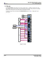
The connections of these links are shown in
MGT Links
:
For MGT Clocking see
Clocks
:
Page 15
Functional Description
ad-ug-1360_v1_0.pdf


