ADM-SDEV-BASE/XCKU060 User Manual
V1.0 - 27th November 2018
3.2 JTAG Interface
3.2.1 On-board Interface
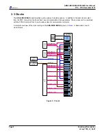
A JTAG boundary scan chain can be accessed via a standard connector on the config FMC (J2). This allows the
connection of the Xilinx JTAG cable for FPGA debug using the Xilinx toolchain.
The JTAG chain starts on the config FMC board and passes through the FPGA, the LPC FMC (J1) (if fitted) and
the FMC+ (J3) (if fitted).
The scan chain is shown in
JTAG Boundary Scan Chain
:
FPGA
XCKU060
LPC
FMC
(J1)
FMC1_PRESENT#
Level Shift
FMC2_VIO –> 3V3
En#
FMC1_TDI
FMC1_TDO
FPGA_TDI
HDR_TDO
Level Shift
3V3 -> FMC2_VIO
FMC2_TDI
FMC2_TDO
Config
FMC
(J2)
FMC+
(J3)
FMC3_PRESENT#
Level Shift
FMC2_VIO –> 3V3
En#
FMC3_TDI
FMC3_TDO
FPGA_TDO
Figure 4 : JTAG Boundary Scan Chain
At each stage the clock signal on this JTAG interface (TCK) has a parallel termination (49.9
Ω
+ 22pF to ground)
located at the far end of the line.
3.2.2 JTAG Voltages
The Vcc supply provided to the JTAG cable on the config FMC is +3.3V and is protected by a poly fuse rated at
375mA.
The JTAG signals on all of the FMC boards use 3.3V signals and are connected through level translators to the
ADM-SDEV-BASE board scan chain.
The voltage level of the JTAG chain on the ADM-SDEV-BASE board is set to the config FMC adjustable voltage
FMC2_VIO.
Page 7
Functional Description
ad-ug-1360_v1_0.pdf


