ADM-PCIE-8V3 User Manual
Figure 13 : GPIO Connector
3.11.1 Direct Connect FPGA Signals
Four nets are broken out to the GPIO header as two differential pairs. These signal are suitable for any 1.8V
supported signaling standards supported by the Xilinx UltraScale architecture. See Xilinx UG571 for IO options.
LVDS and 1.8 CMOS are popular options.
The direct connect GPIO signals are limited to 1.8V by a quickswitch (74CBTLVD3861BQ) in order to protect the
FPGA from overvoltage on IO pins. This quickswitch allows the signals to travel in either direction with only 4
ohms of series impedance and less than 1ns of propagation delay. The nets are directly connected to the FPGA
after the quickswitch.
Direct connect signal names are labeled GP0_1V8_P/N and GP1_1V8_P/N to show polarity and grouping. The
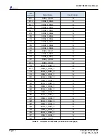
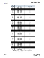
signal pin allocations can be found in
Complete Pinout Table
3.11.2 Low Speed Serial IO
A pin configurable serial buffer transceiver allows for RS232, RS485, and RS422 signal standard support. For
details on configuring the transceiver please reference the IC manufacturer datasheet. Linear Technologies part
number LTC2870. Direct link: http://cds.linear.com/docs/en/datasheet/28701fa.pdf
Signal naming is kept consistent with the Linear Tech datasheet and FPGA pin allocations can be found in the
Complete Pinout Table
. Be sure to constrain and drive each control pin for expected behavior.
3.12 User EEPROM
A 2Kb I2C user EEPROM is provided for storing MAC addresses or other user information. The EEPROM is part
number M24C02-RMC6TG.
The address pins A2, A1, and A0 are all strapped to a logical '0'.
Write protect (WP), Serial Clock (SCL), and Serial Data (SDA) pin assignments can be found in
Complete Pinout
Table
with the names SPARE_WP, SPARE_SCL, and SPARE_SDA respectively.
WP, SDA, and SCL signals all have external pull-up resistors on the card.
Page 19
Functional Description
ad-ug-1308_v1_9.pdf
Содержание ADM-PCIE-8V3
Страница 1: ...ADM PCIE 8V3 User Manual Document Revision 1 9 28th June 2017...
Страница 8: ...ADM PCIE 8V3 User Manual Figure 3 Optional Blower Page 4 PCB Information ad ug 1308_v1_9 pdf...
Страница 24: ...ADM PCIE 8V3 User Manual Page Intentionally left blank Page 20 Functional Description ad ug 1308_v1_9 pdf...


