ADM-PCIE-8V3 User Manual
3.5 QSFP28
Two QSFP28 cages are available at the front panel. Both cages are capable of housing either active optical or
passive copper QSFP28 or QSFP compatible components. The communication interface can run at up to
28Gbps per channel. There are eight channels between the two QSFP28 cages (total maximum bandwidth of
224Gbps). These cages are ideally suited for 8x 25G or 2x 100G Ethernet or any other protocol supported by the
Xilinx GTY Transceivers. Please see Xilinx User Guide UG578 for more details on the capabilities of the
transceivers.
Both QSFP28 cages have control signals connected to the FPGA. Their connectivity is detailed in the
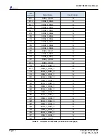
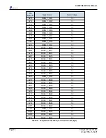
Complete
Pinout Table
at the end of this document. The notation used in the pin assignments is QSFP0 and QSFP1 with
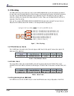
locations clarified in the diagram below.
Use the QSFP*_SEL_1V8_L in conjunction with the OPTICAL_SCL_1V8 and OPTICAL_SDA_1V8 pins as
detailed in
Complete Pinout Table
to communicate with QSFP28 register space.
Note:
The LP_MODE (Low Power Mode) to each QSFP28 cage is pulled up by default. For many high performance
optical transcievers to operate, this pin must be driven low by the FPGA.
Figure 8 : QSFP Locations
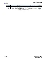
The order options for the ADM-PCIE-8V3 include an option to fit the QSFP28 optical transceivers. The table
below shows the part number for the transceivers fitted with each option.
Order Code
Description
Part Number
Manufacturer
Q10
40G (4x10) QSFP Optical Transceiver
FTL410QE2C
Finisar
Q14
56G (4x14) QSFP Optical Transceiver
FTL414QB2C
Finisar
Q25
100G (4x25) QSFP28 Optical Transceiver
FTLC9551REPM
Finisar
Table 12 : QSFP28 Part Numbers
Page 12
Functional Description
ad-ug-1308_v1_9.pdf
Содержание ADM-PCIE-8V3
Страница 1: ...ADM PCIE 8V3 User Manual Document Revision 1 9 28th June 2017...
Страница 8: ...ADM PCIE 8V3 User Manual Figure 3 Optional Blower Page 4 PCB Information ad ug 1308_v1_9 pdf...
Страница 24: ...ADM PCIE 8V3 User Manual Page Intentionally left blank Page 20 Functional Description ad ug 1308_v1_9 pdf...


