background image

ADM-PCIE-8V3 User Manual


LEDs

Status

Green

Running and no alarms

Green + Red

Standby (Powered off)

Flashing Green + Flashing Red
(together)

Attention - critical alarm active

Flashing Green + Flashing Red
(alternating)

Service Mode

Flashing Green + Red

Attention - alarm active

Red

Missing application firmware or
invalid firmware

Flashing Red

FPGA configuration cleared to
protect board

Table 15 : Status LED Definitions

3.8 SMA Timing Input

All cards are fitted with a U.FL connector that can be utilized as a timing input. This connector can be accessed

with a U.FL cable internal to the chassis, or cabled to an SMA or similar connector at the frton panel. Contact

[email protected] for front panel connector options.

Input is on FPGA pin P30, IOSTANDARD LVCMOS18

The signal is isolated through a optical isolator part number ACPL-M61L with a 739 ohm of series resistance.

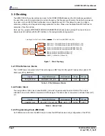
Figure 11 : Timing Input Schematic

Page 16

Functional Description

ad-ug-1308_v1_9.pdf

Содержание ADM-PCIE-8V3

Страница 1: ...ADM PCIE 8V3 User Manual Document Revision 1 9 28th June 2017...

Страница 2: ...without prior written consent from Alpha Data Parallel Systems Ltd Head Office Address 4 West Silvermills Lane Edinburgh EH3 5BD UK Telephone 44 131 558 2600 Fax 44 131 558 2700 email sales alpha data...

Страница 3: ...ence Clocks 9 3 3 PCI Express 11 3 4 DDR4 SDRAM 11 3 5 QSFP28 12 3 6 FireFly 13 3 7 System Monitor 15 3 7 1 System Monitor Status LEDs 15 3 8 SMA Timing Input 16 3 9 USB Front Panel Interface 17 3 10...

Страница 4: ...erature Monitors 15 Table 15 Status LED Definitions 16 Table 16 Complete Pinout Table 21 List of Figures Figure 1 ADM PCIE 8V3 Product Photo 1 Figure 2 Thermal Performance 3 Figure 3 Optional Blower 4...

Страница 5: ...at 2400MT s 32GB option rated at 1866MT s Two QSFP28 zQSFP sites capable of data rates up to 28 Gbps per channel 112 Gbps per cage Two Samtec FireFly sites capable of data rates up to 28 Gbps per cha...

Страница 6: ...r If the application requires a low profile bracket and the order quantity is high contact sales alpha data com to get the correct bracket fitted before shipping 2 2 3 Power Requirements The PCIe Spec...

Страница 7: ...mbient and select User Override for the Effective Theta JA and enter the figure associated with your system LFM in the blank field Proceed to enter all applicable design elements and utilization in th...

Страница 8: ...ADM PCIE 8V3 User Manual Figure 3 Optional Blower Page 4 PCB Information ad ug 1308_v1_9 pdf...

Страница 9: ...FL input for a timing synchronization input a 12 pin header for general purpose use clocking control pins debug etc and low speed serial communications and a robust system monitor XCVU095 2 FFVC1517E...

Страница 10: ...tate ON State SW1 1 OFF User Switch Pin AV27 1 Pin AV27 0 SW1 2 OFF Flash Lockdown Flash block Lockdown enabled Flash block Lockdown disabled SW1 3 OFF Service Mode Regular Operation Firmware update s...

Страница 11: ...Ds Comp Ref Function ON State OFF State D4 DONE FPGA is configured FPGA is not configured D8 USER_LED_G0 User defined 0 pin AT27 User defined 1 pin AT27 D2 USER_LED_G1 User defined 0 pin AU27 User def...

Страница 12: ...z 30ppm Source Si5338 Clock Synth NB6L11S Fanout FireFly 161 1328125MHz Factory Default MGTREFCLK0_126 FireFly 161 1328125MHz Factory Default MGTREFCLK0_125 NB6L11S Fanout Memory Interface Clock 300Mh...

Страница 13: ...8V SCL is at FPGA pin L30 1 8V with external pull ups included The Si5328 input clock comes from FPGA pins M29 and M30 and includes 100 Ohm AC coupled termination on the 1 8V FPGA bank Signal Target F...

Страница 14: ...O Standard P pin N pin MEM_CLK_0 IO_L13_T2L_GC_44 LVDS G31 G32 MEM_CLK_1 IO_L11_T2L_GC_94 DIFF_HSTL_I_18 AN25 AN26 Table 11 Memory Reference Clocks DIFF_TERM_ADV TRUE is required for LVDS termination...

Страница 15: ...ge the mode to Advanced and open the GT Settings tab change the form factor driven insertion loss adjustment from Add in Card to Chip to Chip See Xilinx PG239 for more details 3 4 DDR4 SDRAM Two banks...

Страница 16: ...n the pin assignments is QSFP0 and QSFP1 with locations clarified in the diagram below Use the QSFP _SEL_1V8_L in conjunction with the OPTICAL_SCL_1V8 and OPTICAL_SDA_1V8 pins as detailed in Complete...

Страница 17: ...the pin assignments is FireFly0 and FireFly1 with locations clarified in the diagram below Use the FIREFLY _SEL_1V8_L in conjunction with the OPTICAL_SCL_1V8 and OPTICAL_SDA_1V8 pins as detailed in C...

Страница 18: ...Manufacturer F14 56G 40G 4x14 10 FireFly Optical Transceiver ECUO B04 14 017 0 3 1 1 01 Samtec F28 28G 25G 4x28 25 FireFly Optical Transceiver ECUO B04 28 017 0 3 1 1 01 Samtec Table 13 FireFly Part...

Страница 19: ...e card edge Monitors Index Purpose Description ETC ETC Elapsed time counter seconds EC EC Event counter power cycles 12 0V ADC00 Board Input Supply 3 3V ADC01 Board Input Supply 3 3V ADC02 Board Input...

Страница 20: ...Table 15 Status LED Definitions 3 8 SMA Timing Input All cards are fitted with a U FL connector that can be utilized as a timing input This connector can be accessed with a U FL cable internal to the...

Страница 21: ...ected at the front panel USB port Section 3 10 2 3 10 1 Configuration From Flash Memory The FPGA can be automatically configured at power on from a 1 Gbit BPI flash memory device Micron part number MT...

Страница 22: ...operty BITSTREAM CONFIG OVERTEMPSHUTDOWN Enable current_design set_property CONFIG_MODE BPI16 current_design set_property CFGBVS GND current_design set_property CONFIG_VOLTAGE 1 8 current_design Gener...

Страница 23: ...lete Pinout Table 3 11 2 Low Speed Serial IO A pin configurable serial buffer transceiver allows for RS232 RS485 and RS422 signal standard support For details on configuring the transceiver please ref...

Страница 24: ...ADM PCIE 8V3 User Manual Page Intentionally left blank Page 20 Functional Description ad ug 1308_v1_9 pdf...

Страница 25: ...1 2 E8 DDR4_0_A12 1 2 J11 DDR4_0_A13 1 2 C9 DDR4_0_A14 1 2 B11 DDR4_0_A15 1 2 K12 DDR4_0_A16 1 2 H9 DDR4_0_A17 1 2 G11 DDR4_0_A2 1 2 D11 DDR4_0_A3 1 2 E12 DDR4_0_A4 1 2 G10 DDR4_0_A5 1 2 F10 DDR4_0_A6...

Страница 26: ...1 2 L10 DDR4_0_DQ0 1 2 L9 DDR4_0_DQ1 1 2 M15 DDR4_0_DQ10 1 2 M17 DDR4_0_DQ11 1 2 M14 DDR4_0_DQ12 1 2 N18 DDR4_0_DQ13 1 2 N16 DDR4_0_DQ14 1 2 N17 DDR4_0_DQ15 1 2 F15 DDR4_0_DQ16 1 2 E16 DDR4_0_DQ17 1 2...

Страница 27: ...DQ4 1 2 D18 DDR4_0_DQ40 1 2 B22 DDR4_0_DQ41 1 2 A19 DDR4_0_DQ42 1 2 A18 DDR4_0_DQ43 1 2 C19 DDR4_0_DQ44 1 2 B19 DDR4_0_DQ45 1 2 A22 DDR4_0_DQ46 1 2 C18 DDR4_0_DQ47 1 2 G22 DDR4_0_DQ48 1 2 J20 DDR4_0_D...

Страница 28: ...0_DQ8 1 2 M16 DDR4_0_DQ9 1 2 L12 DDR4_0_DQS0_C 1 2 M12 DDR4_0_DQS0_T 1 2 L14 DDR4_0_DQS1_C 1 2 L15 DDR4_0_DQS1_T 1 2 E13 DDR4_0_DQS2_C 1 2 F13 DDR4_0_DQS2_T 1 2 A15 DDR4_0_DQS3_C 1 2 B15 DDR4_0_DQS3_T...

Страница 29: ...A2 1 2 AU9 DDR4_1_A3 1 2 AT10 DDR4_1_A4 1 2 AL12 DDR4_1_A5 1 2 AM12 DDR4_1_A6 1 2 AM10 DDR4_1_A7 1 2 AL11 DDR4_1_A8 1 2 AP7 DDR4_1_A9 1 2 AV9 DDR4_1_ACT_N 1 2 AR10 DDR4_1_ALERT_N 1 2 AN11 DDR4_1_BA0 1...

Страница 30: ...AL17 DDR4_1_DQ14 1 2 AM13 DDR4_1_DQ15 1 2 AR15 DDR4_1_DQ16 1 2 AP14 DDR4_1_DQ17 1 2 AT15 DDR4_1_DQ18 1 2 AR14 DDR4_1_DQ19 1 2 AH10 DDR4_1_DQ2 1 2 AP17 DDR4_1_DQ20 1 2 AN16 DDR4_1_DQ21 1 2 AN17 DDR4_1...

Страница 31: ...1 2 AW21 DDR4_1_DQ46 1 2 AU19 DDR4_1_DQ47 1 2 AH19 DDR4_1_DQ48 1 2 AJ22 DDR4_1_DQ49 1 2 AH12 DDR4_1_DQ5 1 2 AF21 DDR4_1_DQ50 1 2 AH22 DDR4_1_DQ51 1 2 AF20 DDR4_1_DQ52 1 2 AJ19 DDR4_1_DQ53 1 2 AH21 DD...

Страница 32: ...1 2 AT13 DDR4_1_DQS2_C 1 2 AR13 DDR4_1_DQS2_T 1 2 AV17 DDR4_1_DQS3_C 1 2 AU17 DDR4_1_DQS3_T 1 2 AP22 DDR4_1_DQS4_C 1 2 AN22 DDR4_1_DQS4_T 1 2 AV21 DDR4_1_DQS5_C 1 2 AV22 DDR4_1_DQS5_T 1 2 AH20 DDR4_1...

Страница 33: ...0_RX3_N MGT AE38 FIREFLY0_RX3_P MGT D28 FIREFLY0_SEL_1V8_L 1 8 AM36 FIREFLY0_TX0_N MGT AM35 FIREFLY0_TX0_P MGT AK36 FIREFLY0_TX1_N MGT AK35 FIREFLY0_TX1_P MGT AH36 FIREFLY0_TX2_N MGT AH35 FIREFLY0_TX2...

Страница 34: ...FLASH_A12 1 8 AP29 FLASH_A13 1 8 AN32 FLASH_A14 1 8 AN33 FLASH_A15 1 8 AR29 FLASH_A16 1 8 AR30 FLASH_A17 1 8 AP28 FLASH_A18 1 8 AR28 FLASH_A19 1 8 AK28 FLASH_A2 1 8 AR31 FLASH_A20 1 8 AT31 FLASH_A21...

Страница 35: ...LASH_DQ9 1 8 AV29 FLASH_OE_L 1 8 AW27 FLASH_WAIT 1 8 AV30 FLASH_WE_L 1 8 AR26 FPGA_CPLD_SPARE 1 8 AW23 FPGA_FLASH_RST_L 1 8 F30 GP0_1V8_N 1 8 G30 GP0_1V8_P 1 8 E31 GP1_1V8_N 1 8 E30 GP1_1V8_P 1 8 N34...

Страница 36: ...A6 PCIE_REFCLK_PIN_N MGT_REFCLK AA7 PCIE_REFCLK_PIN_P MGT_REFCLK J1 PCIE_RX0_N MGT J2 PCIE_RX0_P MGT L1 PCIE_RX1_N MGT L2 PCIE_RX1_P MGT AJ1 PCIE_RX10_N MGT AJ2 PCIE_RX10_P MGT AL1 PCIE_RX11_N MGT AL2...

Страница 37: ...PCIE_TX10_PIN_P MGT AM4 PCIE_TX11_PIN_N MGT AM5 PCIE_TX11_PIN_P MGT AP4 PCIE_TX12_PIN_N MGT AP5 PCIE_TX12_PIN_P MGT AT4 PCIE_TX13_PIN_N MGT AT5 PCIE_TX13_PIN_P MGT AU6 PCIE_TX14_PIN_N MGT AU7 PCIE_TX...

Страница 38: ...PUDC_B 1 8 E28 QSFP0_LP_MODE_1V8 1 8 F29 QSFP0_MODPRS_L 1 8 G39 QSFP0_RX0_N MGT G38 QSFP0_RX0_P MGT E39 QSFP0_RX1_N MGT E38 QSFP0_RX1_P MGT C39 QSFP0_RX2_N MGT C38 QSFP0_RX2_P MGT B37 QSFP0_RX3_N MGT...

Страница 39: ..._N MGT H35 QSFP1_TX3_P MGT H33 RA 1 8 L27 RB 1 8 H28 RXEN_L 1 8 L30 SI5328_1V8_SCL 1 8 L29 SI5328_1V8_SDA 1 8 M30 SI5328_REFCLK_IN_N 1 8 Requires DIFFTERM M29 SI5328_REFCLK_IN_P 1 8 Requires DIFFTERM...

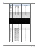
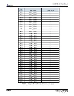
Страница 40: ...l Pin Number Signal Name Bank Voltage H29 TE485 1 8 AD10 TMS 1 8 AT27 USER_LED_G0 1 8 AU27 USER_LED_G1 1 8 AU23 USER_LED_R 1 8 AV27 USR_SW 1 8 Table 16 Complete Pinout Table Page 36 Complete Pinout Ta...

Страница 41: ...locations in PCIe Reference Clocks added note to use pullnone in Clocking added note about SEL pins to QSFP28 and FireFly updated Thermal Performance to use test results 22 Aug 2016 1 5 K Roth Update...

Страница 42: ...inburgh EH3 5BD UK Telephone 44 131 558 2600 Fax 44 131 558 2700 email sales alpha data com website http www alpha data com Address 611 Corporate Circle Suite H Golden CO 80401 Telephone 303 954 8768...

Отзывы: