SERIES IP503 INDUSTRIAL I/O PACK EIA/TIA-232E & CENTRONICS COMMUNICATION MODULE
___________________________________________________________________________________________
- 7 -
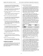
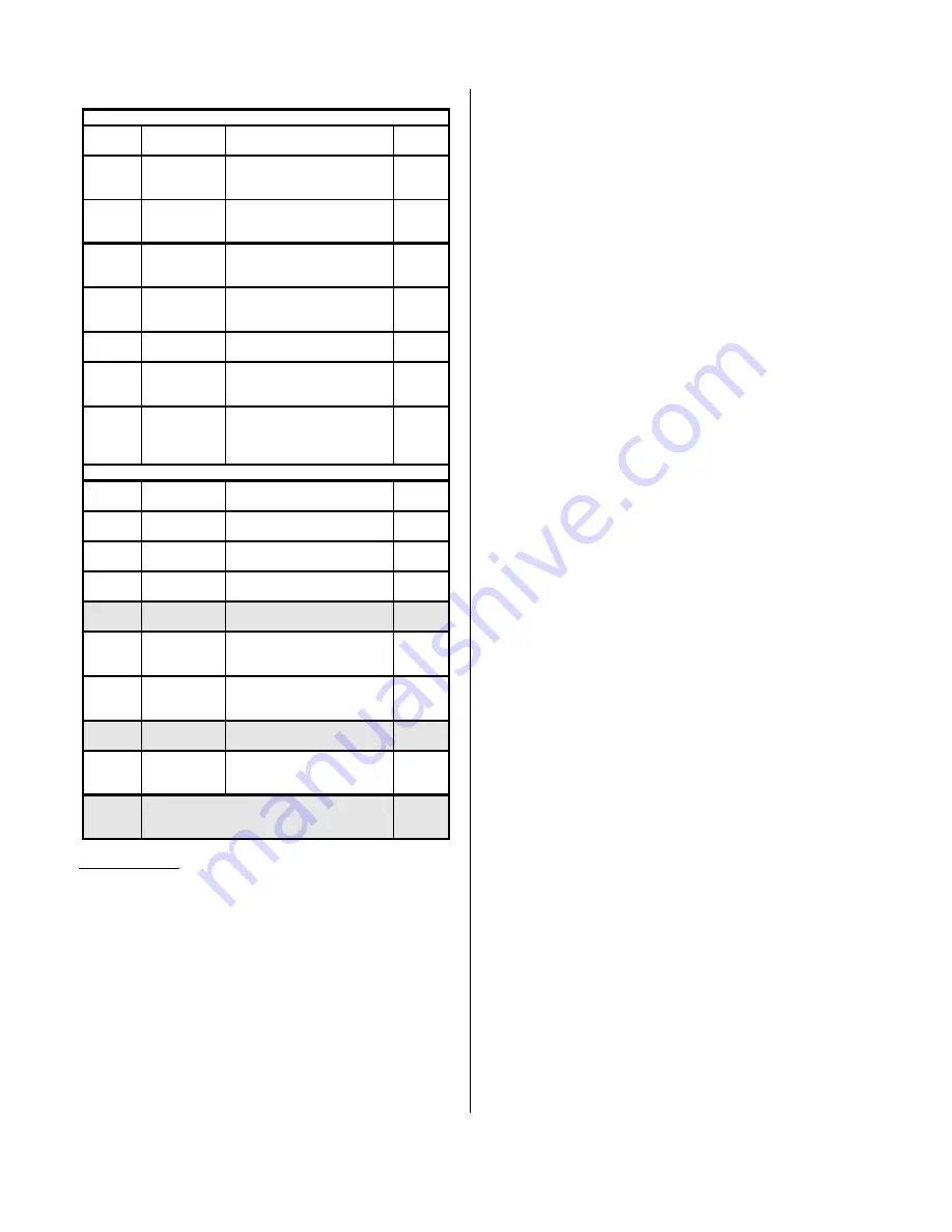
Serial Port B Registers continued:
Base
Addr+
MSB
D15D08
LSB
D07 D00
Base
Addr+
14
Not Driven
1
READ - IIR
Port B Interrupt
Identification Register
15
14
Not Driven
1
WRITE - FCR
Port B FIFO Control
Register
15
16
Not Driven
1
R/W - LCR
Port B Line Control
Register
17
18
Not Driven
1
R/W - MCR
Port B Modem Control
Register
19
1A
Not Driven
1
R/W - LSR
Port B Line Status Register
1B
1C
Not Driven
1
R/W - MSR
Port B Modem Status
Register
1D
1E
Not Driven
1
R/W - SCR
Port B Scratch
Pad/Interrupt Vector
Register
1F
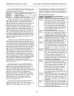
Centronics Parallel Port Registers
Base
Addr+
MSB
D15D08
LSB
D07 D00
Base
Addr+
20
Not Driven
1
READ/WRITE - LPT
Line-Printer Data Port
21
22
Not Driven
1
READ ONLY - LPS
Line-Printer Status
23
24
Not Driven
1
READ/WRITE - LPC
Line-Printer Control
25
26
Not Driven
1
INVALID
(NOT USED
2
)
27
28
Not Driven
1
R/W - LEM
Line Printer
Extended Mode Select
29
2A
Not Driven
1
R/W - LIM
Line Printer
Interrupt Mode Select
2B
2C
Not Driven
1
INVALID
(NOT USED
2
)
2D
2E
Not Driven
1
R/W - LIV
Line Printer
Interrupt Vector Register
2F
30
↓
7E
NOT USED
2
31
↓
7F
Notes (Table 31):
1 The upper 8 bits of these registers are not driven and pullups
on the carrier data bus will cause these bits to read high (1’s)
2 The IP will not respond to addresses that are "Not Used"
3 All I/O Reads and writes are 2 wait states, except ID PROM
reads which are 1 wait state
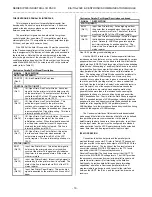
This board operates in two different modes. In one mode,
this device remains software compatible with the industry
standard 16C450 family of UART’s and provides double-buffering
of data registers. In 16C450 mode, holding and shift registers
eliminate the need for precise synchronization between the host
CPU and the serial data. In the FIFO mode (enabled via bit 0 of
the FCR register), data registers are FIFO-buffered so that read
and write operations can be performed while the UART is
performing serial-to-parallel and parallel-to-serial conversions
Two FIFO modes are possible: FIFO Interrupt Mode and FIFO
Polled Mode. Some registers operate differently between the
available modes and this is noted in the following paragraphs
RBR - Receiver Buffer Register, Ports A & B (READ Only)
The Receiver Buffer Register (RBR) is a serial port input data
register that receives the input data from the receiver shift
register and holds from 5 to 8 bits of data, as specified by the
character size programmed in the Line Control Register (LCR bits
0 & 1)If less than 8 bits are transmitted, then data is right-justified
to the LSB. If parity is used, then LCR bit 3 (parity enable) and
LCR bit 4 (type of parity) are required. Status for the receiver is
provided via the Line-Status Register (LSR)When a full character
is received (including parity and stop bits), the data-received
indication bit (bit 0) of the LSR is set to 1The host CPU then
reads the Receiver Buffer Register, which resets LSR bit 0 to 0If
the character is not read prior to a new character transfer
between the receiver shift register and the receiver buffer
register, the overrun-error status indication is set in LSR bit 1If
there is a parity error, the error is indicated in LSR bit 2If a stop
bit is not detected, a framing error indication is set in bit 3 of the
LSR
Serial asynchronous data is input to the receiver shift register
via the receive data line (RxD)From the idle state, this line is
monitored for a high-to-low transition (start bit)When the start bit
is detected, a counter is reset and counts the 16x clock to 7-1/2
(which is the center of the start bit)The start bit is judged valid if
RxD is still low. This is known as false start bit detection. By
verifying the start bit in this manner, it helps to prevent the
receiver from assembling an invalid data character due to a low-
going noise spike on RxD. If the data on RxD is a symmetrical
square wave, the center of the data cells will occur within
±
3125%
of the actual center (providing an error margin of 46875%)Thus,
the start bit can begin as much as one 16x clock cycle prior to
being detected
THR - Transmitter Holding Register, Ports A & B (WRITE
Only)
The Transmitter Holding Register (THR) is a serial port output
data register that holds from 5 to 8 bits of data, as specified by
the character size programmed in the Line Control Register. If
less than 8 bits are transmitted, then data is entered right-justified
to the LSB. This data is framed as required, then shifted to the
transmit data line (TxD)In the idle state, TxD is held high. In
Loopback Mode, this data is looped back into the Receiver Buffer
Register
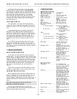
DLL & DLM - Divisor Latch Registers, Ports A & B (R/W)
The Divisor Latch Registers form the divisor used by the
internal baud-rate generator to divide the 8MHz system clock to
produce an internal sampling clock suitable for synchronization to
the desired baud rate. The output of the baud generator (RCLK)
is sixteen times the baud rate. Two 8-bit divisor latch registers
per port are used to store the divisors in 16-bit binary format. The
DLL register stores the low-order byte of the divisor, DLM stores
the high-order byte. These registers must be loaded during
initialization
Note that bit 7 of the LCR register must first be set high to
access the divisor latch registers (DLL & DLM) during a read/write
operation


