


E-2
Service Guide
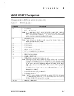
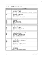
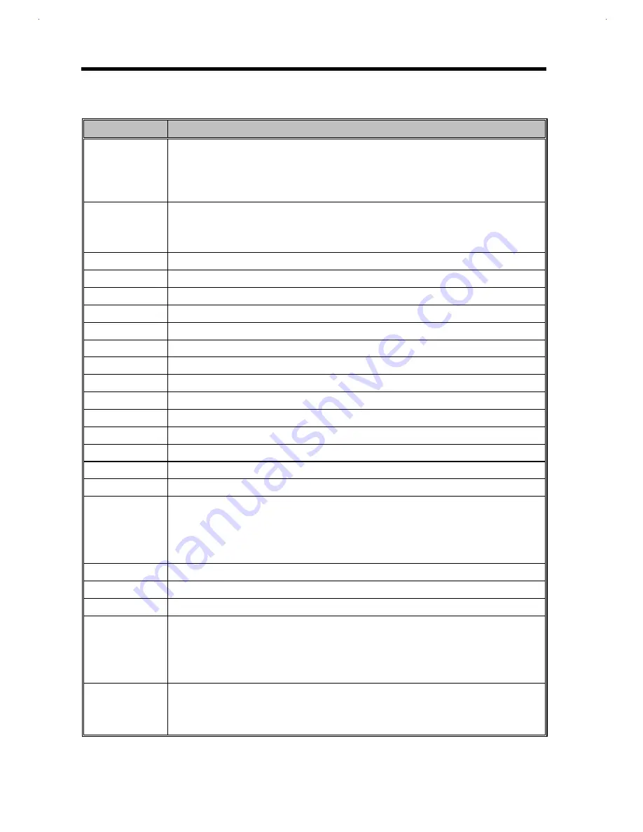
Table E-1
POST Checkpoint List (Continued)
Checkpoint
Description
2Ch
•
128K base memory testing
•
Set default SS:SP= 0:400
Note: The 128K base memory area is tested for POST execution. The remaining
memory area is tested later.
20h
•
KB controller(8041/8042) testing
•
KB type determination
•
Write default command byte upon KB type
24h
•
PIC(8259) testing & initialization
30h
•
System Shadow RAM
34h
•
DRAM sizing
3Ch
•
Initialize interrupt vectors
4Bh
•
Identify CPU brand and type
35h
•
PCI pass 0
40h
•
Assign I/O if device request
41h
•
Assign Memory if device requested
44h
•
Assign IRQ if device request
45h
•
Enable command byte if device is OK
51h
•
DownLoad keyboard matrix
50h
•
Initialize Video display
4Ch
•
ChipUp initialization for CPU clock checking
54h
•
Process VGA shadow region
58h
•
Set POST screen mode(Graphic or Text)
•
Display Acer(or OEM) logo if necessary
•
Display Acer copyright message if necessary
•
Display BIOS serial number
5Ch
•
Memory testing
5Ah
•
SMRAM test and SMI handler initialization
4Eh
•
Audio initialization
60h
•
External Cache sizing
•
External Cache testing(SRAM & Controller)
•
Enable internal cache if necessary
•
Enable external cache if necessary
64h
•
Reset KB device
•
Check KB status
Note: The keyboard LEDs should flash once.
Содержание AcerNote Light 370P
Страница 1: ...TI Extensa 61X Series AcerNote 370P Notebook Service Guide PART NO 2238309 0809 DOC NO PRINTED IN USA ...
Страница 6: ...vi ...
Страница 26: ...1 8 Service Guide Figure 1 5 Main Board Layout Bottom Side ...
Страница 49: ...System Introduction 1 31 1 5 1 3 Power Management Figure 1 14 Power Management Block Diagram ...
Страница 55: ...System Introduction 1 37 1 6 System Block Diagram Figure 1 15 System Block Diagram ...
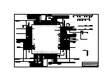
Страница 64: ...Major Chips Description 2 7 2 2 5 Pin Diagram Figure 2 4 M1521 Pin Diagram ...
Страница 99: ...2 42 Service Guide 2 5 3 Pin Diagram Figure 2 10 C T 65550 Pin Diagram ...
Страница 116: ...Major Chips Description 2 59 2 6 4 Block Diagram Figure 2 11 Functional Block Diagram 16 bit PC Card Interface ...
Страница 117: ...2 60 Service Guide Figure 2 12 Functional block diagram CardBus Card Interface ...
Страница 118: ...Major Chips Description 2 61 2 6 5 Pin Diagram Figure 2 13 PCI to PC Card 16 bit terminal assignments ...
Страница 119: ...2 62 Service Guide Figure 2 14 PCI to CardBus terminal assignments ...
Страница 135: ...2 78 Service Guide 2 7 3 Pin Diagram Figure 2 16 NS87336VJG Pin Diagram ...
Страница 145: ...2 88 Service Guide 2 8 2 Pin Diagram Figure 2 17 YMF715 Block Diagram ...
Страница 185: ...Disassembly and Unit Replacement 4 5 Figure 4 3 Disassembly Sequence Flowchart ...
Страница 209: ...B 2 Service Guide ...
Страница 210: ...Exploded View Diagram B 3 ...
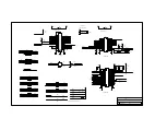
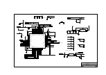
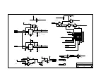
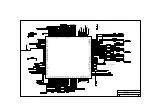
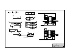
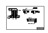
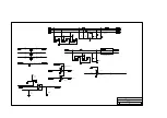
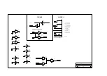
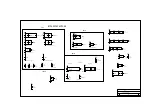
Страница 217: ...A p p e n d i x D A p p e n d i x D Schematics This appendix shows the schematic diagrams of the notebook ...


