


2-50
Service Guide
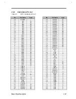
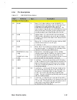
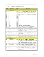
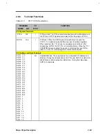
Table 2-10
C&T 65550 Pin Descriptions (continued)
Pin#
Pin Name
Type
Description
PCI Bus Interface (continued)
90
91
92
93
94
95
96
97
98
CA0 (P16)
CA1 (P17)
CA2 (P18)
CA3 (P19)
CA4 (P10)
CA5 (P21)
CA6 (P22)
CA7 (P23)
CA8 (BLANK)
Out
Out
Out
Out
Out
Out
Out
Out
I/O
Address bus for DRAM C.
CA0-7 may be configured as flat panel data output (P16-23).
See also pins 71-88 (in Flat Panel Display interface pin
descriptions section).
CA8 may be configured as VAFC BLANK# out or vertical
reference input (VREF) for video capture.
99
HREF
In
Horizontal reference input for video capture.
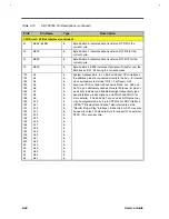
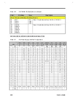
156
RASA# (RASAB0#)
Out
RAS for DRAM A (or bank 0 in 2MB configurations)
123
RASB# (RASAB1#)
Out
RAS for DRAM B (or bank 1 in 2MB configurations)
101
RASC# (VRDY)
(KEY)
Out
In
RAS for DRAM C (or color key input from external PC-Video
source or VAFC "Video System Ready" input)
160
CASAL#
Out
CAS for the DRAM A lower byte
159
CASAH#
Out
CAS for the DRAM A upper byte
126
CASBL#
Out
CAS for the DRAM B lower byte
125
CASBH#
Out
CAS for the DRAM B upper byte
104
CASCL# (WECL#)
(VR6/VP14)
I/O
DRAM C low byte CAS (or video in red-6 or VAFC VP14)
103
CASCH# (CASC#)
(VR7/VP15)
I/O
DRAM C high byte CAS (or video in red-7 or VAFC VP15)
157
WEA# (WEAH#)
(WEAB0#)
Out
Write enable for DRAM A (or bank 0 in 2MB)
124
WEB# (WEBH#)
(WEAB1#)
Out
Write enable for DRAM B (or bank 1 in 2MB)
102
WEC# (WECH#)
(PCLK)
Out
Write enable for DRAM C (or video in port PCLK out)
155
OEAB0#
Out
Output enable for DRAMs A and B, bank 0, 1 of 2MB
100
OEC#
(VCLK)
Out
In
Output enable for DRAM C (or VAFC "Video Input Clock" if
DRAM C not used)
Содержание AcerNote Light 370P
Страница 1: ...TI Extensa 61X Series AcerNote 370P Notebook Service Guide PART NO 2238309 0809 DOC NO PRINTED IN USA ...
Страница 6: ...vi ...
Страница 26: ...1 8 Service Guide Figure 1 5 Main Board Layout Bottom Side ...
Страница 49: ...System Introduction 1 31 1 5 1 3 Power Management Figure 1 14 Power Management Block Diagram ...
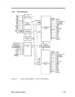
Страница 55: ...System Introduction 1 37 1 6 System Block Diagram Figure 1 15 System Block Diagram ...
Страница 64: ...Major Chips Description 2 7 2 2 5 Pin Diagram Figure 2 4 M1521 Pin Diagram ...
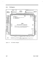
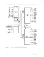
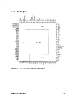
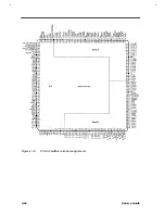
Страница 99: ...2 42 Service Guide 2 5 3 Pin Diagram Figure 2 10 C T 65550 Pin Diagram ...
Страница 116: ...Major Chips Description 2 59 2 6 4 Block Diagram Figure 2 11 Functional Block Diagram 16 bit PC Card Interface ...
Страница 117: ...2 60 Service Guide Figure 2 12 Functional block diagram CardBus Card Interface ...
Страница 118: ...Major Chips Description 2 61 2 6 5 Pin Diagram Figure 2 13 PCI to PC Card 16 bit terminal assignments ...
Страница 119: ...2 62 Service Guide Figure 2 14 PCI to CardBus terminal assignments ...
Страница 135: ...2 78 Service Guide 2 7 3 Pin Diagram Figure 2 16 NS87336VJG Pin Diagram ...
Страница 145: ...2 88 Service Guide 2 8 2 Pin Diagram Figure 2 17 YMF715 Block Diagram ...
Страница 185: ...Disassembly and Unit Replacement 4 5 Figure 4 3 Disassembly Sequence Flowchart ...
Страница 209: ...B 2 Service Guide ...
Страница 210: ...Exploded View Diagram B 3 ...
Страница 217: ...A p p e n d i x D A p p e n d i x D Schematics This appendix shows the schematic diagrams of the notebook ...


