


User Manual
This document is not allowed to
transmit without ZTE Corporation
’s
permission
©ZTE CORPORATION All rights reserved
25
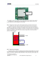
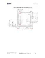
Figure 4-7 SIM card circuit reference design diagram
NOTE
:
(1)
The SIM card PCB wiring should be laid closely around the module as much as possible.
(2)
The VSIM, CLK, DATA and RST signals should be enveloped by the ground wires. The position of 33pF
capacitance should be reserved on CLK, DATA and RST signals wiring and the position should be
close to the SIM card socket to prevent the interference sources from affecting the SIM card’s
reading/writing.
(3)
Since the ESD components are very close to the SIM card socket, it’s recommended to add TVS
components on 4-CH SIM card signals, meanwhile, the signal wires need go through TVS component
before entering the module’s baseband processor during the layout to avoid damaging the module.
(4)
The width of VSIM power wiring should be above 6mil at least (recommended to use 8mil).
(5)
The
filter capacitance of VSIM power wiring adopts 1uf (the value can’t be larger than 10uf or
smaller than 1uf), and then 0.1uf capacitance is added.
4.4
Audio interf ace
MG2639_V3 module provides audio input and output interfaces through its PINs. There are 2
Speaker interfaces and 2 Microphone interfaces. Only one pair I/O works at the same time. See the
audio interface circuit in figure 4-8.