
User Manual
This document is not allowed to
transmit without ZTE Corporation
’s
permission
©ZTE CORPORATION All rights reserved
20
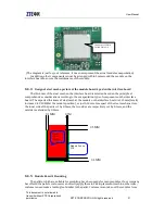
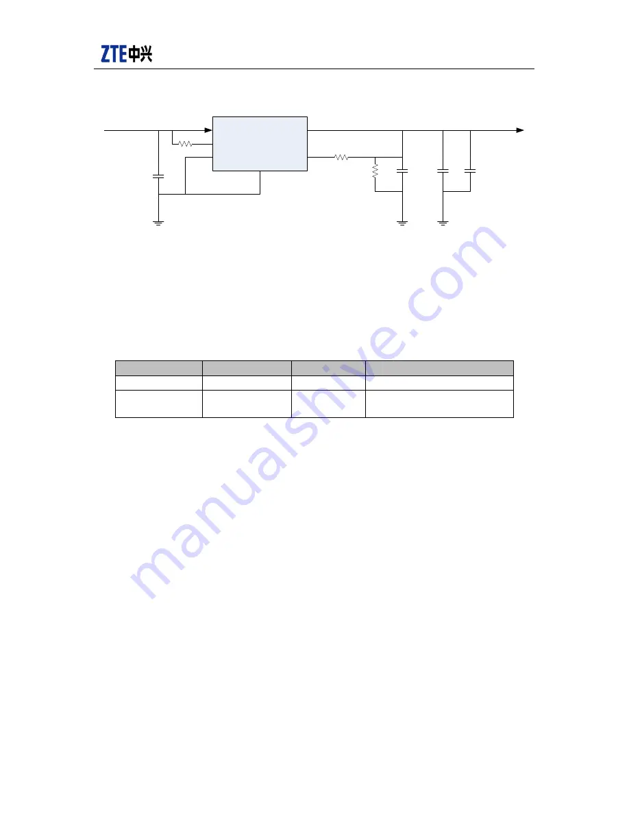
Figure 4-2 Power reference circuit
R5
2.2K
R6
1K
C6
0.1uF
C8
100uF
C7
0.1uF
R4
10K
C5
10uF
D1
MIC29302
GND
TAB
/SHUT
IN
OUT
SENSE
输入电压
输出模块用电压
VBAT
Power design
MG2639_V3 module is powered by VBAT. If the external power cannot be stably started, it’s
recommended to add buffer circuit in the circuit. See the module’s required voltage characteristics in
table 4-1.
Table 4-1 Voltage characteristics
Classification
Vmin
Typical
Vmax
Input voltage
3.4V
3.8V
4.2V
Input current
1mA
--
300mA
(
Depends on the network
signal
)
The module is very strict with the requirements on the power supply and grounding:
(1). The filtering must be performed on the power and grounding, and the power ripple must be
controlled under 50Mv. Do not power any other part in the system because it might affect the RF
performance.
(2). Select the power cables with at least 80mil traces during the layout and keep the integrality
of ground line.
(3). Make sure the Max. instantaneous output current is larger than 2A if the Max. input current
is very high.
Power on
The module is under power-off status after it’s normally powered on. To turn on the module,
provide a 2s-5s low level pulse to the PWRKEY_N PIN. If one 1K resistance is connected with the
PWRKEY_N PIN, the module can be automatically powered on after connected to the power supply.
Power off
To turn off the module, use AT command “AT+ZPWROFF” or provide a 2s~5s low level pulse to
the PWRKEY_N PIN.
Reset
Use the above method to firstly “power-off” and then “power-on” to hard reset the module.
If the external reset function has to be used, provide a low level pulse lasting at least 500ms to the
SYSRST_N PIN within 2 seconds after the module is turned on. Before that, the external MCU_RESET
signal must be kept at low level. See the reset circuit design in figure 4-1.
Suspend the SYSRST_N PIN if not used.