42
Tyros2
MO
TR
OWNE
BEDIE
MODE
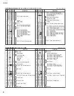
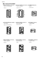
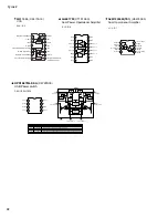
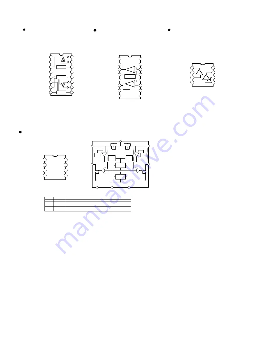
NJM12904M(TE1)
(X5475A00)
Dual Operational Amplifier
1
2
3
4
8
7
6
5
Output A
+V
Non-Inverting
Input A
Ground
+DC Voltage
Supply
Output B
Inverting
Input B
Non-Inverting
Input B
Inverting
Input A
+
-
+
-
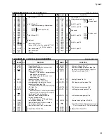
LA6517M
(XT131A00)
Dual Power Operational Amplifier
1
2
3
4
5
6
7
8
16
15
14
13
12
11
10
9
Thermal Shut
Doun and
Current Limiter
Amp1
Amp2
NC
NC
OUT 1
VCC
OUT 2
VEE
NC
NC
NC
NC
INPUT -2
INPUT +2
INPUT +1
INPUT -1
NC
NC
1
2
3
4
5
6
7
8
9
10
11
12
13
14
15
16
OUT1
IN1
VDD
NC
NC
IN2
OUT2
Balance/Indivdual
Volume control
Refarence Voltage
Filter
NC
GND
Volume/Volume2 control
Noise reduction
Balance/VOLUME2
Pass/VCA Switching
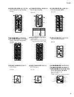
M51132L
(XE470A00)
VCA
Switching
Controled
Voltage
Regulater
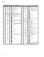
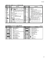
UPD16875G-E2-A
(X4722A00)
USB Power switch
1
2
3
4
8
7
6
5
CTL1
CTL2
FLG1
FLG2
OUT1
OUT2
IN
GND
PIn No.
1/4
2/3
6
7
8/5
Pin Name
CTL1/CTL2
FLG1/FLG2
GND
IN
OUT1/OUT2
Pin Function
Control input: Active-low, TTL input
Detection flag (output): Active-low,Nch open-drain
Ground
Power input: Source of MOSFET for output. Power supply to internal circuitry of IC.
Switch output: Drain of MOSFET for output. Usually, connected to load.
Reference
voltage
Overcurrent
detection block
Gate
control
Overvoltage
lockout circuit
Thermal
shutdown circuit
8
OUT1
(Output 1)
IN (Input)
Reference
voltage
Overcurrent
detection block
2
6
FLG1
(Flag output 1)
GND
1
CTL1
(Control input 1)
4
CTL2
(Control input 2)
4 FLG2
(Flag output 2)
5 OUT2
(Output 2)
Gate
control
Overvoltage
lockout circuit
Thermal
shutdown circuit
7


