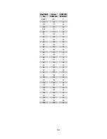
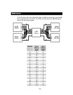
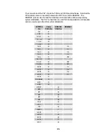
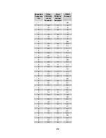
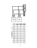
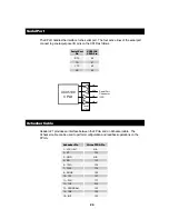
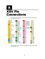
24
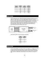
Switch
Virtex
FPGA Pin
XC95108
CPLD Pin
Flash RAM
Function
SW1
174
SW2
175
SW3
176
SW4
185
7
DIPSW1
161
50
A13
DIPSW2
159
52
A14
DIPSW3
155
53
A15
DIPSW4
153
54
A16
DIPSW5
149
55
A17
DIPSW6
146
56
A18
DIPSW7
142
58
A19
DIPSW8
140
59
A20
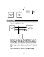
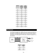
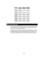
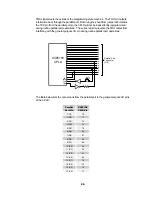
Digit and Bargraph LEDs
The XSV Board has a 10-segment bargraph LED and two more 7-segment LED digits for
use by the FPGA and CPLD. All of these LEDs are active-high meaning that an LED
segment will glow when a logic-high is applied to it.
The table below lists the connections from the FPGA and CPLD to the LEDs. The LEDs
also share the same pins as the uppermost eight bits of the Flash RAM address bus. If
the Flash RAM is programmed with several FPGA bitstreams, then the DIP switch can be
used to select a particular bitstreams which will be loaded into the FPGA by the CPLD.
Summary of Contents for XSV
Page 8: ...7...
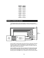
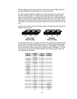
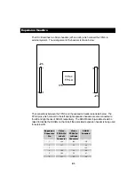
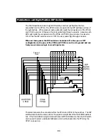
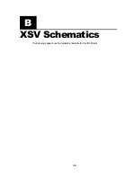
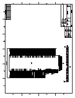
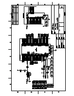
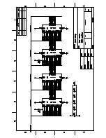
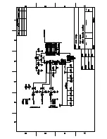
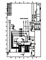
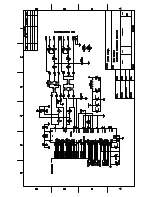
Page 34: ...33 B XSV Schematics The following pages show the detailed schematics for the XSV Board...
Page 35: ......
Page 36: ......
Page 37: ......
Page 38: ......
Page 39: ......
Page 40: ......
Page 41: ......
Page 42: ......
Page 43: ......
Page 44: ......
Page 45: ......
Page 46: ......
Page 47: ......
Page 48: ......
Page 49: ......
Page 50: ...XSV Board V0 1 Layout...