
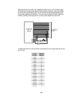

17
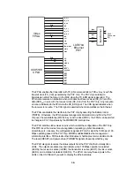
with the PIXELCLK generated by the FPGA. The FPGA lowers the /BLANK signal when
the pixels fall outside the desired visible area of the monitor screen.
The colormap of the RAMDAC is initialized by the FPGA using the D bus along with the
RS, /WR, and /RD signals. The 24-bit colormap entries are passed in groups of three
bytes over the eight-bit D bus synchronized by the /WR signal. The register-select signals
(RS0, RS1, RS2) select the staging register for writing the colormap. The contents of the
staging register are written into the colormap after the last byte of color information arrives
over the D bus, and then the internal colormap address is incremented to point to the next
entry.
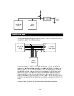
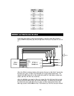
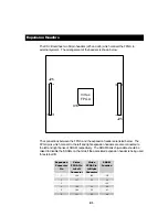
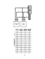
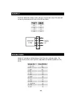
The shunt placement to enable the FPGA to generate VGA signals directly or through the
RAMDAC is shown below.
J7
J7
J5
J5
J6
J6
Direct VGA
Shunt Setting
RAMDAC
Shunt Setting
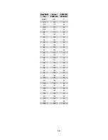
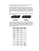
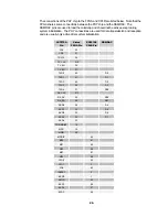
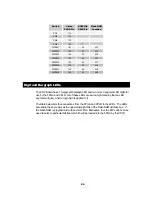
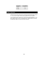
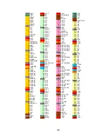
The pin assignments for the connection of the FPGA to the VGA signal generation circuitry
are shown below. Note that the FPGA shares some connections between the RAMDAC
and the chip which interfaces to the Ethernet (LXT970A). The RAMDAC pins are used to
load the colormap and should not be active except during system initialization. The other
connections are used for Ethernet data transmission and reception and are usually only
active after system initialization.
Direct
VGA Pin
RAMDAC
Pin
Virtex
FPGA Pin
LXT970A
Function
PIXELCLK
52
/HSYNC
/HSYNC
48
/VSYNC
/VSYNC
49
/BLANK
50
RED0
P0
70
RED1
P1
71
GREEN0
P2
72
GREEN1
P3
73
BLUE0
P4
74
BLUE1
P5
78
P6
79
P7
80
/RD
47
/WR
46
RS0
31
TXD4
RS1
28
RX_ER
RS2
26
RX_DV
D0
42
TXD0
D1
41
TXD1
Summary of Contents for XSV
Page 8: ...7...
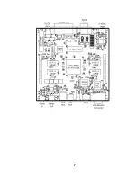
Page 34: ...33 B XSV Schematics The following pages show the detailed schematics for the XSV Board...
Page 35: ......
Page 36: ......
Page 37: ......
Page 38: ......
Page 39: ......
Page 40: ......
Page 41: ......
Page 42: ......
Page 43: ......
Page 44: ......
Page 45: ......
Page 46: ......
Page 47: ......
Page 48: ......
Page 49: ......
Page 50: ...XSV Board V0 1 Layout...