
14
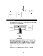
SRAM Banks
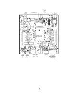
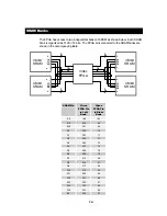
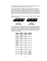
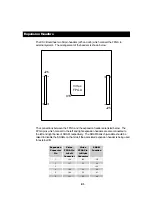
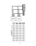
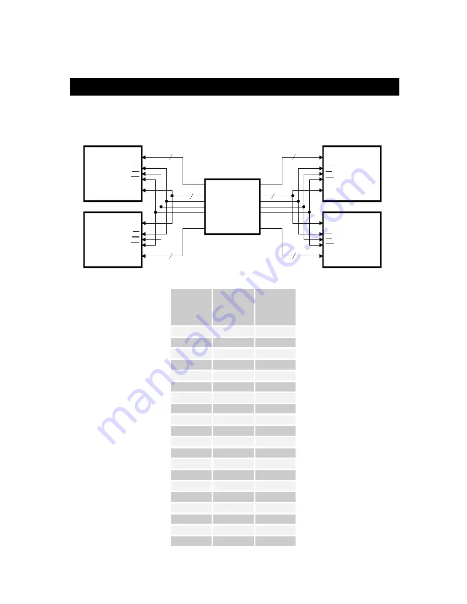
The FPGA has access to two independent banks of SRAM as shown below: Each SRAM
bank is organized as 512K
×
16 bits. The FPGA pins connected to the SRAM banks are
shown in the accompanying table.
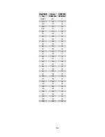
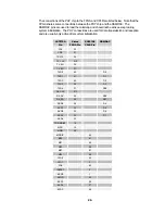
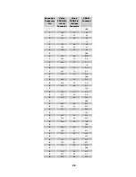
SRAM Pin
Virtex
FPGA Pin
to Left
Bank
Virtex
FPGA Pin
to Right
Bank
/CE
186
109
/OE
228
95
/WE
201
68
D0
202
70
D1
203
71
D2
205
72
D3
206
73
D4
207
74
D5
208
78
D6
209
79
D7
215
80
D8
216
81
D9
217
82
D10
218
84
D11
220
85
D12
221
86
D13
222
87
D14
223
93
D15
224
94
A0
200
67
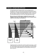
Virtex
FPGA
19
8
8
4 Mbit
SRAM
4 Mbit
SRAM
we
we
oe
oe
ce
ce
19
8
8
4 Mbit
SRAM
d
0 - 7
a
0 - 1 8
4 Mbit
SRAM
a
0 - 1 8
a
0 - 1 8
a
0 - 1 8
d
0 - 7
d
0 - 7
d
0 - 7
we
we
oe
oe
ce
ce
Summary of Contents for XSV
Page 8: ...7...
Page 34: ...33 B XSV Schematics The following pages show the detailed schematics for the XSV Board...
Page 35: ......
Page 36: ......
Page 37: ......
Page 38: ......
Page 39: ......
Page 40: ......
Page 41: ......
Page 42: ......
Page 43: ......
Page 44: ......
Page 45: ......
Page 46: ......
Page 47: ......
Page 48: ......
Page 49: ......
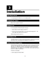
Page 50: ...XSV Board V0 1 Layout...