
21
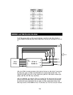
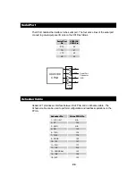
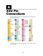
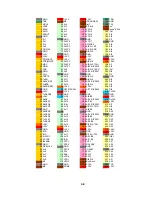
Expansion Headers
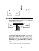
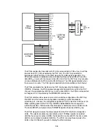
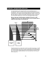
The XSV Board has two 50-pin headers (J25 and J26) which connect the FPGA to
external systems. The arrangement of the headers is shown below:
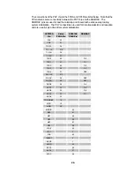
The connections between the FPGA and the expansion headers are listed below. The
FPGA pins which connect to the left and right expansion headers are also connected to
the left and right banks of SRAM, respectively. The SRAM bank chip-enable should be
raised to disable the SRAMs on that side if the associated expansion header is being used
for external I/O.
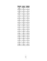
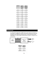
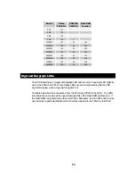
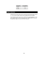
Expansion
Connector
Pin
Virtex
FPGA Pin
to Left
Connector
Virtex
FPGA Pin
to Right
Connector
SRAM
Function
1
186
109
/CE
2
187
53
A9
3
+5V
4
188
54
A8
5
189
55
A7
6
191
56
A6
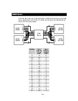
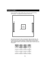
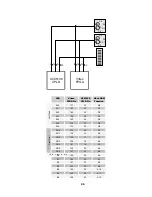
J26
J25
U18
Virtex
FPGA
1
1
4
9
4
9
5
0
5
0
2
2
Summary of Contents for XSV
Page 8: ...7...
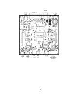
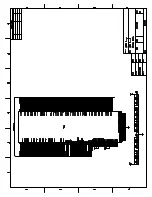
Page 34: ...33 B XSV Schematics The following pages show the detailed schematics for the XSV Board...
Page 35: ......
Page 36: ......
Page 37: ......
Page 38: ......
Page 39: ......
Page 40: ......
Page 41: ......
Page 42: ......
Page 43: ......
Page 44: ......
Page 45: ......
Page 46: ......
Page 47: ......
Page 48: ......
Page 49: ......
Page 50: ...XSV Board V0 1 Layout...