


Carrier Board Design Guide for SOM-9X35 Module
4
2.
General Carrier Board Recommendations
This section contains general guidelines for the PCB stack-up and the layout of traces. The general guide lines
for routing style, topology, and trace attribute recommendations are also discussed.
2.1 PCB Stack-Up
The PCB stack-up consists of signal layers and reference (power and ground) layers. The signal layers are
referred to as the component layer (top), inner layer and solder layer (bottom).
The carrier board designers can choose between two basic categories of PCB stack-up design: micro strip and
strip line. Microstrip designs have the outer signal layers exposed while stripline designs have the outermost
signal layers shielded by reference layers.
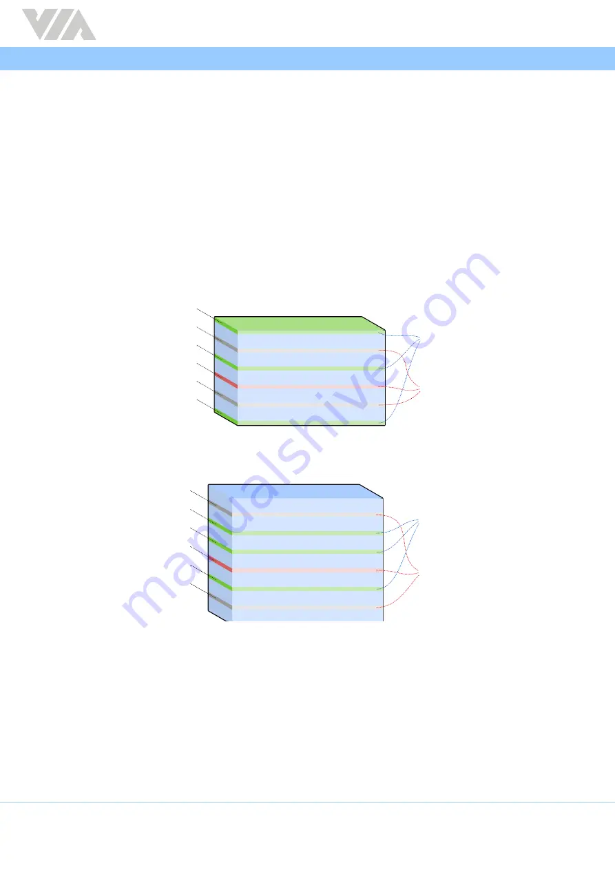
The following figures show examples of microstrip and stripline designs.
Microstrip Stack-Up Design
Signal layers
Reference layers
Component layer
Ground layer
Inner layer
Power layer
Ground layer
Solder layer
Figure 02:
Microstrip PCB stack-up example
Stripline Stack-Up Design
Signal layers
Reference layers
Inner layer
Ground layer
Inner layer
Power layer
Ground layer
Inner layer
Figure 03:
Stripline PCB stack-up example
The choice of microstrip or stripline design depends on the application for which the carrier board is being
designed. If the carrier board is being designed for locations where sensitivity to EMI is an issue, a stripline
design is recommended for reducing EMI and noise coupling. For applications where the tolerance for EMI
levels is greater, a microstrip design is recommended to reduce costs. Due to the inherent nature of stripline
PCB stacks, broad-side coupling is possible.