
USSI Microlok II Functional description
UM-6800A Rev1.3 July 2005 Page 11 of 27
is assumed to be the maximum high voltage or minimum low voltage
depending on which would cause the worse case for reliability and safety
considerations.
Response times for railway and transit application have historically been
specified in the 100msec to 1second range. The response times for Microlok
II, based on older products, allows for fast response to state changes while
allowing filtering time for reliability reasons. In addition, it must be
recognized that some processing may be delayed by other system tasks. In
cases where such delays can impact system safety, such as delivery of
outputs within 200msec or reading of inputs within 400msec, the maximum
tolerable delay time is specified in the requirements.
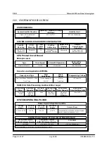
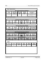
Non-Vital I /O Board
The Non-Vital I/O board is designed to receive non-vital inputs (controls) and
generate non-vital outputs (indications). The version of the NV.IN32.OUT32
board connects each of its 32 inputs and outputs to a 96-pin connector
mounted on the rear of the board. The board employs polyswitches to protect
the output circuitry. A polyswitch functions like an auto circuit breaker.
When the over current trip point (about 0.75 amp) is exceeded, the device
switches to high impedance. The polyswitch returns to low impedance when
the overload or short circuit condition is removed. Inputs on the boards are
activated from a positive voltage relative to battery ground over a range of 6
to 30V DC. The non-vital I/O boards use latch ICs to buffer inputs and field
effect transistors to drive outputs.
•
The minimum ON threshold for a Non-Vital Input will be 4.5V DC for
nominal 24V DC systems.
•
The maximum OFF threshold for a Non-Vital Input will be 2V DC for
nominal 24V DC systems.