background image

USSI                                                                                                                  Microlok II Functional description


 UM-6800A Rev1.3                                           July 2005                                                         Page 9 of 27 

• 

Responding  to  CPU  board  front  panel  switch  inputs  and  operating  the 
associated displays 

• 

Interacting  with  a  laptop  PC  during  system  diagnostic  operations, 
application logic programming, and executive software upgrading 

4.1.5.  POWER SUPPLY BOARD


The Power supply board will have double width housed in the card file and it 
operates in the range of 9.5V to 16.5V DC producing 5V at 3amps and +12V 
at 1amp that are needed for the operation of the card file circuitry. The power 
supply  will  have  a  start–up  voltage  requirement  of  11.5V  DC.  This  prevents 
the  unit  from  attempting  a  recovery  when  battery  voltage  is  low.  The  power 
supply board performs the following functions: 

• 

Converts the external supply voltage (9.8V to 16.2V DC) to reg12V 
and +5 for outputs to the system card file internal circuits 

• 

Supplies energy to the VCOR relay coil under the control of the CPU board 

The  power  supply  board  serves  a  vital  role  in  the  fail-safe  design  of  the 
Microlok  II  system.  The  regulated  +12V  and  +5V  power  is  distributed  to  all 
system card file boards through the card file back plane bus.  

Summary of Contents for Microlok II

Page 1: ... INDIA HEREINAFTER USSI FURNISHED TO YOU ON THE FOLLOWING CONDITIONS NO RIGHT OR LICENSE IN RESPECT TO THIS DOCUMENT OR ITS CONTENTS IS GIVEN OR WAIVED IN SUPPLYING THE DOCUMENT TO YOU THIS DOCUMENT OR ITS CONTENTS ARE NOT TO BE USED OR TREATED IN ANY MANNER INCONSISTENT WITH THE RIGHTS OF USSI AND ARE NOT TO BE COPIED REPRODUCED DISCLOSED TO OTHERS OR DISPOSED OF EXCEPT WITH THE PRIOR WRITTEN CON...

Page 2: ......

Page 3: ...uly 2004 Title of Author Design Engineer This Issue Approved By G Perumalsamy Date 19 July 2004 Title of Approver Design Manager DOCUMENT CHANGE RECORD Issue No Reason For Change Date of Revision 1 0 Draft for review 27 July 2004 1 1 Internal review comments 04 October 2004 1 2 Initial Issue to SECR 12 October 2004 1 3 Board Diagrams added 04 July 2005 ...

Page 4: ...________________________________ 17 5 1 SERIAL I O________________________________________________________________ 17 5 1 1 MICROLOK PROTOCOL ____________________________________________________ 18 5 1 2 GENISYS PROTOCOL______________________________________________________ 19 6 1 MICROLOK II SOFTWARE ____________________________________________________ 19 6 1 1 EXECUTIVE SOFTWARE ________________...

Page 5: ...OG ______________________________________________________ 23 10 1 2 SYSTEM ERROR LOG______________________________________________________ 23 10 1 3 SYSTEM USER DATA LOG__________________________________________________ 23 10 1 4 SYSTEM MERGED EVENT LOG______________________________________________ 23 11 1 SYSTEM SPECIFICATION __________________________________________________ 24 ...

Page 6: ...ive software during run time The high level block diagram of the Microlok II system is shown below The system uses diversity and self checking concepts in which critical operations are performed in diverse ways using diverse software operations and critical system hardware is tested with self checking operations Permissive outputs are allowed only if the results of diverse logic operations corresp...

Page 7: ...n vital control Panel Operator VDU functions Serial I O channels for communicating with MLK II to MLK II MLK II to CAB Other Non Vital application Maintenance and Diagnostic function 4 1 MICROLOK II HARDWARE The Microlok II system consists of modular card file mounted equipment and external peripheral devices that are used to interface the card file circuitry to the field gears and other associate...

Page 8: ...ttery voltage is low Nominal 24V input output boards will have an input output supply in the range of 19 6V DC to 32 4V DC 4 1 3 CARDFILE The Microlok II card file is a G64 96 bus based card file that holds the CPU Power Supply Variety of I O boards The card file will be a user configurable The Microlok II card file is designed to house standard 6UX220 Euro card plug in printed circuit boards The ...

Page 9: ...ing has an internal EEPROM that is used to store site specific configuration data Even if the CPU board is replaced the configuration data remains intact within the CPU connector s EEPROM Ports 1 and 2 support an RS 485 hardware interface Port 3 supports an RS 423 RS 232 interface Port 4 5 supports an RS 232 interface Figure 2 ADJUST UP DOWN REJECT ACTION ACCEPT RESET DOWN UP L R M E N 68332 CPU O...

Page 10: ...s and options 3 A B C D E Yellow LEDs Reserved for serial link status 4 1 2 3 4 5 6 7 8 Red LEDs User defined in application software 5 ON LINE Green LED When lit indicates normal system operation successful diagnostics 6 VPP ON Yellow LED When lit indicates FLASH 5V or 12V programming voltage enabled via board jumper 7 RESET Green LED When lit indicates that the system is in reset mode 8 RESET Mo...

Page 11: ... that are needed for the operation of the card file circuitry The power supply will have a start up voltage requirement of 11 5V DC This prevents the unit from attempting a recovery when battery voltage is low The power supply board performs the following functions Converts the external supply voltage 9 8V to 16 2V DC to regulated 12V and 5 for outputs to the system card file internal circuits Sup...

Page 12: ... not lit refer CPS CLEAR FUNCTION details in Figure 3 4 4 1 6 PHYSICAL I O The Physical I O characteristics have been chosen to accommodate normal railway and transit interface devices Requirements for standard 24V DC battery supply Vital and Non Vital relays lamps and LED indications have all been taken into account in determining voltage and current limits The voltage and current ranges specifie...

Page 13: ...irements Non Vital I O Board The Non Vital I O board is designed to receive non vital inputs controls and generate non vital outputs indications The version of the NV IN32 OUT32 board connects each of its 32 inputs and outputs to a 96 pin connector mounted on the rear of the board The board employs polyswitches to protect the output circuitry A polyswitch functions like an auto circuit breaker Whe...

Page 14: ...e connected from outputs to battery negative The high side switch is used to connect battery to the output Each output is protected with a polyswitch which acts like an auto circuit breaker When the over current trip point is reached approximately 0 75A the polyswitch switches to a high impedance state The switch resets to its low impedance state when the additional load or short is removed A shor...

Page 15: ...rop Each Vital Output PCB is having 16 outputs Each output is assigned to the final relay which is driving the outdoor signalling gears such as HR DR in case of signal WNR WRR in case of points Since the output boards are driving outdoor gears they are continuously monitored by the CPU and any abnormal voltage present in the output will lead to system reset shutdown to ensure safety Figure 5 OUT16...

Page 16: ...providing feedback to the processor to ensure that the output is indeed what was requested by processor Also to check the integrity of the feedback loop the outputs are cycled on a periodic basis If an output is currently turned on the processor will turn it off for an instant and verify the correct response from the monitor Failure of these checks would result in a system shutdown and reset See t...

Page 17: ...pective input is turned on 2 IN9 IN16 green LEDs Monitor state of vital inputs 9 through 16 When lit indicates respective input is turned on Vital Inputs Vital inputs which are in most cases derived from the battery supply must have the same range of inputs as the supply battery To ensure reliable operation the Minimum ON thresholds the levels above which an input must read ON were chosen to match...

Page 18: ...ng of any input results in a more restrictive condition All individual input interface circuits on a given board are forced to the more restrictive state through the closed loop vital input monitors The inputs are then read and verified that they can in fact be forced to the more restrictive state This is ensure that no interface circuit malfunction have occurred that could place an input in a les...

Page 19: ...dress select PCB is used for non vital boards 4 1 9 KEYING PLUG Each of the Microlok II card file slots includes a 12 way female keying guide next to the 96 pin connector The guide is used to ensure installation of the proper circuit board in each card file slot after the complete card file board configuration has been determined Each board is equipped with a corresponding 12 way male keying guide...

Page 20: ...t Boolean Bit defined for each Serial Station The Stale Data Time Out SDTO for the Microlok protocol will have an allowable range of 0 100 to 25 000 seconds in 100 millisecond increments This time out will be reset each time a valid message is received This information is included in the Application Configuration At the expiration of the SDTO all input bits for the Serial Station will be set to 0 ...

Page 21: ...em Status Variable will be cleared Input values will not be affected This function will be Non Vital The allowable range for the Polling Interval Timer will be 0 to 2 000 seconds in 10 millisecond increments This Non Vital information will be included in the Application Configuration The allowable range for the No Response Timer will be 30 to 25000 milliseconds in 10 millisecond increments This No...

Page 22: ...nuously executed and controlled from the CPU board in order to detect and act upon various fault conditions Microlok II uses diversity and self checking concepts in which critical operations are performed in diverse ways using diverse software operations and hardware is tested with self checking operations Permissive outputs are allowed only if the results of diverse logic operations correspond an...

Page 23: ... capable of operating in seven different modes 8 1 1 NORMAL MODE In this mode all outputs and application processing are active All other system functions are available at user request This will be the default mode for systems operations in the absence persistent of Critical Errors 8 1 2 SELECTIVE SHUTDOWN MODE This mode will be entered when persistent Critical Errors prohibit complete system oper...

Page 24: ...olean logic the system will include table processing and block processing The system supports Break Before Make execution of Boolean logic equations All Boolean Variables used as operands in the logic equation will be Logic Triggers for the equation and a change in state of any of the operands causes the equation to be evaluated A type of logic processing similar to a traditional computer program ...

Page 25: ...ecords only those events that the user specifies The user data log enables users to monitor a specifically chosen set of events These events are assigned in the configuration section of the Tools program The system then records in the log any state changes of the assigned events along with the date and time that each state changes occurs This log is capable of recording up to 90 000 of the most re...

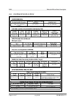
Page 26: ...ile Vibration ENVIRONMENTAL 5 1000 Hz Humidity Limit 95 non condensing 40 C to 70 C All Units CPU Printed Circuit Board Up to 8 megabytes Executive and Application EPROMs 21 MHz Clock Speed Four Intel Micron TE28F800CV B90 Flash Type Capacity and Type Motorola MC68332 Microprocessor Type Operations 4M x 16 1 wait state Total Code Space Clock Speed 21 MHz 32 bits wide 5V and 12V Programming Voltage...

Page 27: ...4V Part No US S Max OFF Voltage 1 5V 100 BATT V 1V Voltage Min ON BATT Voltage V Load Resistance Range Range Output Specifications BATT Part No N17061602 US S Range 24V Voltage V Voltage Max OFF Load Resistance Input Specifications Range Voltage Min ON 16 0V 12 0V or less 62V Non Vital I O Printed Circuit Boards N17061501 Part No US S 6 0 to 30 0V DC 32 Externally Available Externally Inputs 32 Ou...

Page 28: ...USSI Microlok II Functional description Page 26 of 27 July 2005 UM 6800A Rev1 3 NOTES ...

Page 29: ...USSI Microlok II Functional description UM 6800A Rev1 3 July 2005 Page 27 of 27 ...

Reviews: