TSW1200
6 V Input
Ground
D
7
ADC
D1
D16
D4
D3
D2
DCM
USB
Lit when 6V
present
Lit after FPGA
reset completed
Flashes when clock
from ADC present
Lit during
USB access
Flashes while
200 MHz osc present
LitwhenFPGA
finishesloadingbitfile
6 V I/O
3.4
Input Connections
3.4.1
Samtec LVDS Connector
www.ti.com
Hardware Configuration
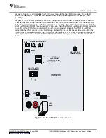
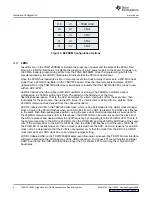
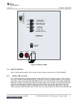
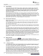
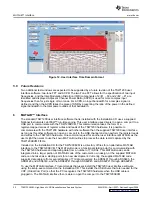
Figure 4. Position of LEDs
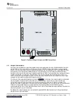
Figure 5 illustrates the position of the various input and output connections on the TSW1200EVM.
The connection between the TSW1200EVM and the ADC EVM to be tested is through a 120-pin Samtec
connector. Fourteen LVDS data pairs plus two LVDS clock pairs have a defined position in the connector
pinout that is common between the TSW1200EVM and many TI ADC EVMs. For the parallel LVDS DDR
data format, the bit clock runs at the same rate as the sample clock to the ADC. For the serial LVDS data
format, the bit clock runs at a higher multiple of the ADC sample clock and is used to strobe the serial
data into the TSW1200EVM and then deserialize the data. For the serial LVDS data format, a second
clock is provided, called the frame clock or FCLK, that runs at the sample rate and is used to delineate the
SLAU212A – April 2007 – Revised August 2008
TSW1200EVM: High-Speed LVDS Deserializer and Analysis System
9


