TSW1200
+6 V
Input
Ground
PROGRAM
RESET
PROM RESET
SW2
SW3
SW5
J
1
7
J10
J11
J16
JP8
J22
o
p
e
n
USB EEPROM
(Default Shorted)
JTAG TDI => TDO
Selects FPGA bit file
from EEPROM
(Default CFG1 for
Parallel DDR format)
(Default Shorted)
6 V I/O
J1
J12
SW4
www.ti.com
Hardware Configuration
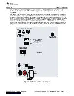
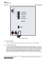
Jumper J17 can be used to disable the 1.2-V power regulator for the FPGA core logic. The default
position for this jumper is to be left uninstalled or open, and in normal operation, this jumper is left
uninstalled.
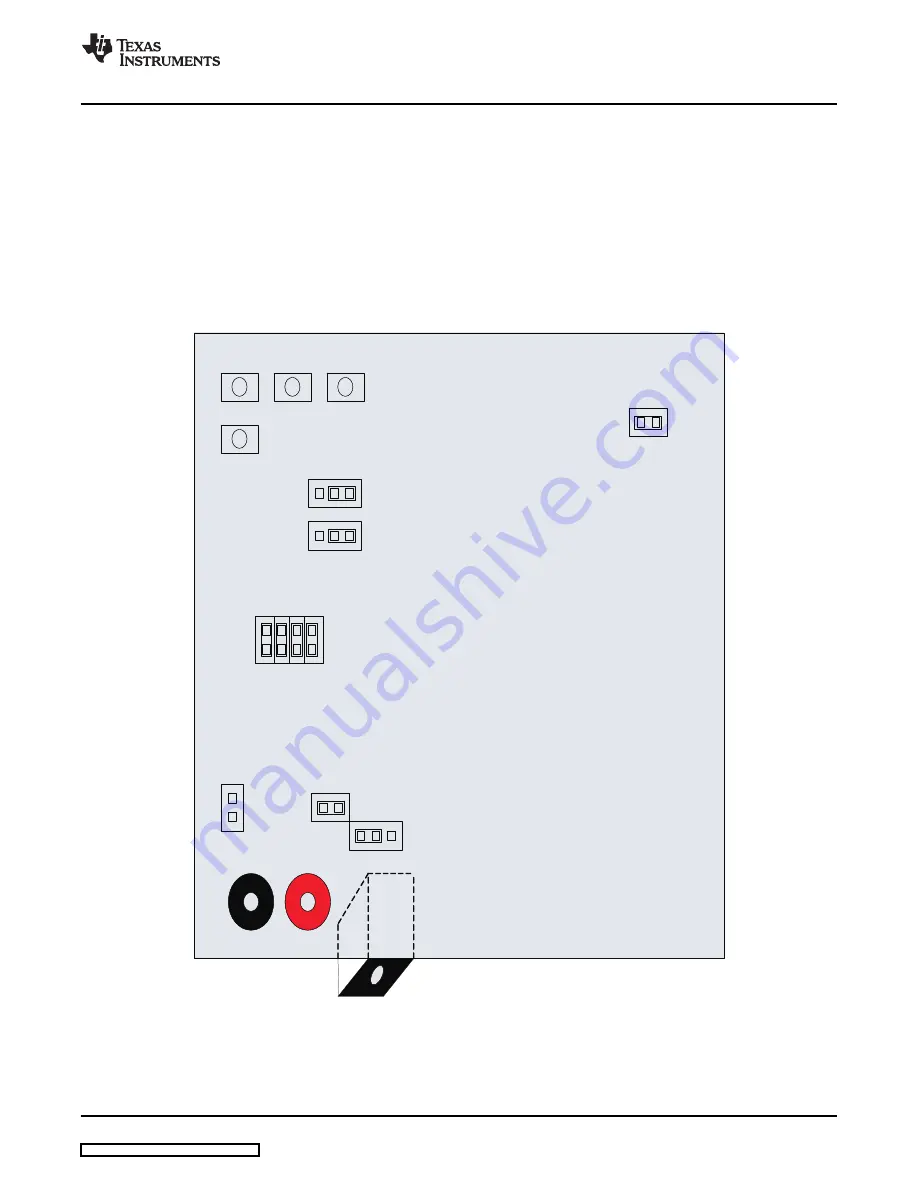
Jumpers J1 and J12 form part of a JTAG chain through the FPGA and the FPGA EEPROM. A chain of
JTAG devices form a loop, with the TDO from one JTAG device connected to the TDI of the next JTAG
device. The normal setting of the JTAG jumpers is to connect the TDI of the JTAG connector to the TDI
pin of the FPGA EEPROM through jumper J12 pins 2-4. Then, the TDO of the FPGA EEPROM connects
to the TDI of the FPGA through jumper J12 pins 1-3 and jumper J1 pins 2-4. The TDO of the FPGA
connects to the JTAG connector pin TDO through jumper J1 pins 1-2. If it desired to remove either the
PFGA or the FPGA EEPROM from the JTAG chain, the jumpers J1 or J12 can be turned 90 degrees to
connect pins 1-2 and 3-4. See the TSW1200EVM schematics and layout sections for illustration of this
option.
Figure 2. Position of Switches and Jumpers
SLAU212A – April 2007 – Revised August 2008
TSW1200EVM: High-Speed LVDS Deserializer and Analysis System
7


