3.2
Switches and Jumpers
3.2.1
Pushbuttons
3.2.2
Jumpers
Hardware Configuration
www.ti.com
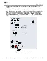
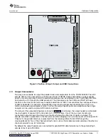
Four pushbutton switches are mounted on the TSW1200EVM. Two pushbutton switches currently have
defined functions; two of the switches are reserved for future use.
The PROGRAM pushbutton (SW3) causes the FPGA to reload its bit file from the FPGA EEPROM on the
TSW1200EVM. The EEPROM currently is large enough to hold two FPGA bit files. When the FPGA loads
a bit file, it loads the bit file indicated by the position of the jumpers J11 and J10. When power is first
applied to the TSW1200EVM, the FPGA also loads its bit file from the EEPROM as determined by the
jumpers J11 and J10. Therefore, pressing the PROGRAM pushbutton has the same effect as
power-cycling the FPGA. All register settings in the FPGA and any data held in the FPGA are lost on
loading the bit file, and the FPGA then is in its initial default configuration.
The RESET (SW4) pushbutton causes the FPGA to clear the FIFO storage, but does not clear any of the
register settings in the FPGA. Any configuration of the FPGA done through register operations such as
setting the UART baud rate will persist after pushing the RESET pushbutton. FPGA register settings only
are cleared by pressing the PROGRAM pushbutton. For this reason, the RESET pushbutton has limited
utility in this revision of the TSW1200EVM; this pushbutton may have more utility defined for it in future
revisions of the FPGA firmware.
The PROM RESET (SW2) is reserved for future use, as is pushbutton SW5.
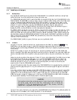
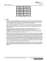
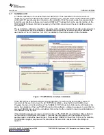
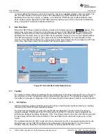
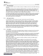
Jumpers J10 and J11 select the bit file to be programmed into the FPGA as indicated in
. The
EEPROM is currently large enough to contain two complete programming files for the FPGA, with
provision to later install a larger EEPROM with the capability to store four complete programming bit files
for the FPGA.
Bit file CFG1 (jumper J10 set to LO and jumper J11 set to HI) is defined for use with ADC EVMs that
employ a parallel LVDS DDR (dual-data rate) format. Bit file CFG2 is defined for use with ADC EVMs that
employ a serialized data format, whether a one-wire serial format or a two-wire serial format. See Figure
3.
Simply moving the position of the jumpers J10 and J11 has no immediate effect. The FPGA does not load
its programming bit file except on initial power up or until the PROGRAM pushbutton is pressed. To
change the operation of the TSW1200EVM for use with a parallel DDR format or with a serial LVDS
format, the jumpers J10 and J11 must be set to the desired position, and then the board must be
power-cycled or have the PROGRAM button pushed.
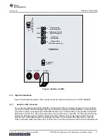
Jumper JP8 selects whether the power supply to the TSW1200EVM is to be supplied by the external 6-V
power module through power jack J7 or by an external 6-V bench power supply through the red banana
jack J15.
A low drop-out linear power regulator on the TSW1200EVM generates a clean, low-noise 5-V supply from
the 6-V power that is input to the TSW1200EVM. The jumper J22 can be used to connect this onboard
regulated 5 V to the red banana jack J15 as an output. This option is a convenience for use with ADC
EVMs that require a single 5-V supply input. In this way, the TSW1200EVM and ADC EVM combination
can be powered completely from the laptop-style 6-V external power supply.
CAUTION
It is possible to select the red banana jack J15 as an input to be connected to a
6-V bench supply and at the same time install jumper J22 to connect the
regulated 5 V to the red banana jack as an output. This, however, over time
causes the 5-V regulator on the TSW1200 to fail.
Jumper J16 is used at the factory to program the small EEPROM for the USB port. The default position for
this jumper is to be installed, and in normal operation, J16 is left installed.
6
TSW1200EVM: High-Speed LVDS Deserializer and Analysis System
SLAU212A – April 2007 – Revised August 2008


