


Signal Multiplex Logic
23
SPRUII5A – December 2017 – Revised November 2018
Copyright © 2017–2018, Texas Instruments Incorporated
DRA77xP/DRA76xP-ACD CPU EVM Board
4
Signal Multiplex Logic
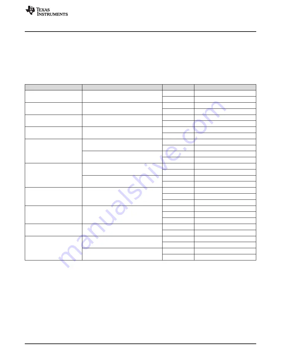
Due to the high level of multiplexing on the SoC (16+ levels), multiplex control logic is required in order to
use the same SoC pins with their various functionality. The information shown in
provides
descriptions of the EVM mux logic.
An I2C-based IO expander is used to control the on-board muxes.
shows the specific bit(s)
assigned to each mux, as well as the specific settings for the various selections.
Table 15. On-Board Mux Setting/Control
MUX
Control Bits
Value
Mux Setting
A
N/A
N/A
NOR Memory (requires mod)
N/A
QSPI Memory (default)
H
(RU18)
EXP3.P1
(VIN6_SEL_S0)
'0'
MCA3/7 to AIC/COMQ8-BT
'1'
Signals to Expansion (default)
M
(RU19)
EXP3.P0
(PM_OEn)
'0'
I2C2 to Power Measurement
'1'
DDC to HDMI Port (default)
K
(RU23)
EXP2.P16
(SEL_UART3_SPI2) '0'
'0'
UART3 to COMQ8/BT
'1'
SPI2 to Expansion (default)
L
(RU22, RU24, RU25)
EXP2.P3
(SEL_I2C3_CAN2)
'0'
DCAN2/MCAN to CAN-FD
'1'
I2C3 to Displays (default)
EXP2.P5
(SEL_EXP_I2C3_DCAN2)
'0'
DCAN2/I2C3 to Expansion
'1'
DCAN2/I2C No Expansion
B
(RU13, RU16, RU7)
EXP2.P0
(SEL_GPMC_AD_VID_S0)
'0'
VOUT3B to FPD-Link Display
'1'
GPMC NOR/NAND (default)
SW6.P[2:1]
OFF/ ON
GPMC to NAND (Bootable)
ON/ OFF
GPMC to NOR (Bootable)
D
(RU8, RU4)
EXP3.P[6,2]
(VIN2_S2, VIN2_S0)
'01'
VIN2A to LI Camera
'10'
VIN2A to Expansion
‘11’
Open (default)
F
(RU15)
EXP3.P[12:11]
(EXVIN2_S2, EXVIN2_S0)
'01'
VIN2A-Upper* to LI Camera
'10'
VIN2A-Upper* to Expansion
‘11’
RGMII1 to Gig PHY (default)
J
(RU14, RU17)
EXP2.P4
(SEL_ENET_MUX_S0)
'0'
VIN4B/GPIO to Expansion
'1'
RGMII0 to Gig PHY (default)
C
(RU5)
SW6.[3]
OFF
GPMC to NOR
ON
MMC2 to eMMC
EXP3.P[15:14]
'00'
eMMC Memory
'11'
Memory selected by SW6.3