background image

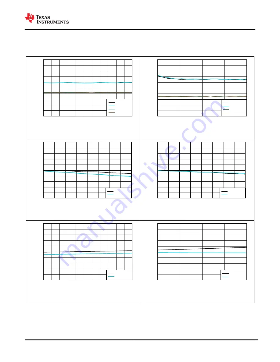
6.17 Typical Characteristics: Voltage Output (continued)

at T

A

 = 25°C, V

DD

 = 5.5 V, external reference = 5.5 V, gain = 1x, 12-bit resolution, and DAC outputs unloaded (unless 

otherwise noted)

Temperature (

C)

V

oltage Ou

tput D

NL (LS

B)

-40

-25

-10

5

20

35

50

65

80

95

110 125

-1

-0.8

-0.6

-0.4

-0.2

0

0.2

0.4

0.6

0.8

1

CH1 MAX
CH0 MAX
CH1 MIN
CH0 MIN


Figure 6-10. Voltage Output DNL vs Temperature

Supply Voltage (V)

V

oltage Ou

tput D

NL (LS

B)

1.8

2.725

3.65

4.575

5.5

-1

-0.8

-0.6

-0.4

-0.2

0

0.2

0.4

0.6

0.8

1

CH1 MAX
CH0 MAX
CH1 MIN
CH0 MIN


Figure 6-11. Voltage Output DNL vs Supply Voltage

Code

V

oltage Ou

tput TUE (

%

FSR)

0

512

1024

1536

2048

2560

3072

3584

4095

-1.5

-1.2

-0.9

-0.6

-0.3

0

0.3

0.6

0.9

1.2

1.5

Channel 1
Channel 0

Internal reference, gain = 4x

Figure 6-12. Voltage Output TUE vs Digital Input Code

Code

V

oltage Ou

tput TUE (

%

FSR)

0

512

1024

1536

2048

2560

3072

3584

4095

-1.5

-1.2

-0.9

-0.6

-0.3

0

0.3

0.6

0.9

1.2

1.5

Channel 1
Channel 0


Figure 6-13. Voltage Output TUE vs Digital Input Code

Temperature (

C)

V

oltage Ou

tput TUE (

%

FSR)

-40

-25

-10

5

20

35

50

65

80

95

110 125

-1.5

-1.2

-0.9

-0.6

-0.3

0

0.3

0.6

0.9

1.2

1.5

Channel 1
Channel 0

DAC channels at midscale

Figure 6-14. Voltage Output TUE vs Temperature

Supply Voltage (V)

V

oltage Ou

tput TUE (

%

FSR)

1.8

2.725

3.65

4.575

5.5

-1.5

-1.2

-0.9

-0.6

-0.3

0

0.3

0.6

0.9

1.2

1.5

Channel 1
Channel 0

DAC channels at midscale

Figure 6-15. Voltage Output TUE vs Supply Voltage

www.ti.com

DAC53202, DAC63202

SLASF47 – MAY 2022

Copyright © 2022 Texas Instruments Incorporated

Submit Document Feedback

15

Product Folder Links: 

DAC53202


DAC63202

Summary of Contents for DAC 3202 Series

Page 1: ... to analog converters DACs The DACx3202 devices support Hi Z power down mode and Hi Z output during power off conditions The DAC outputs provide a force sense option for use as a programmable comparator and current sink The multifunction GPIO function generation and NVM enable these smart DACs for processor less applications and design reuse These devices automatically detect I2C PMBus and SPI int...

Page 2: ...cal Characteristics Current Output 19 6 19 Typical Characteristics Comparator 23 6 20 Typical Characteristics General 24 7 Detailed Description 25 7 1 Overview 25 7 2 Functional Block Diagram 25 7 3 Feature Description 26 7 4 Device Functional Modes 27 7 5 Programming 44 7 6 Register Map 52 8 Application and Implementation 70 8 1 Application Information 70 8 2 Typical Application 70 9 Power Supply...

Page 3: ...r SCL for address configuration Section 7 5 2 2 1 For SDI this pin does not need to be pulled up or pulled down This pin can ramp up before VDD 8 SDA SCLK Input Output Bidirectional I2C serial data bus or SPI clock input This pin must be connected to the IO voltage using an external pullup resistor in I2C mode This pin can ramp up before VDD 9 NC NC No connection Leave the pin unconnected 10 NC NC...

Page 4: ...pins 2 500 1 JEDEC document JEP155 states that 500 V HBM allows safe manufacturing with a standard ESD control process 2 JEDEC document JEP157 states that 250 V CDM allows safe manufacturing with a standard ESD control process 6 3 Recommended Operating Conditions over operating free air temperature range unless otherwise noted MIN NOM MAX UNIT VDD Positive supply voltage to ground AGND 1 7 5 5 V V...

Page 5: ...re coefficient 4 Between end point codes 32d to 4064d for 12 bit resolution 8d to 1016d for 10 bit resolution 0 0008 FSR C Full scale error 4 6 1 7 V VDD 2 7 V DAC at full scale 1 1 FSR 2 7 V VDD 5 5 V DAC at full scale 0 5 0 5 Full scale error temperature coefficient 4 DAC at full scale 0 0008 FSR C OUTPUT Output voltage Reference tied to VDD 0 VDD V CL Capacitive load 2 RL infinite phase margin ...

Page 6: ...5 5 V 0 35 µV Hz Internal VREF gain 4x f 1 kHz DAC at midscale VDD 5 5 V 0 9 Power supply rejection ratio ac 3 Internal VREF gain 4x 200 mV 50 Hz or 60 Hz sine wave superimposed on power supply voltage DAC at midscale 68 dB Code change glitch impulse 1 LSB change around midscale including feedthrough 10 nV s Code change glitch impulse magnitude 1 LSB change around midscale including feedthrough 15...

Page 7: ... to peak 0 1 Hz to 10 Hz DAC at midscale VDD 5 5 V 250 µA output range 150 nAPP Output noise density f 1 kHz DAC at midscale VDD 5 5 V 250 µA output range 1 nA Hz Power supply rejection ratio ac 3 250 µA output range 200 mV 50 Hz or 60 Hz sine wave superimposed on power supply voltage DAC at midscale 0 65 LSB V POWER IDD Current flowing into VDD 3 4 Normal operation DACs at full scale 25 µA output...

Page 8: ...d for 10 years of continuous operation 4 mV OUTPUT Input voltage VREF connected to VDD FBx resistor network connected to ground 0 VDD V VREF connected to VDD FBx resistor network disconnected from ground 0 VDD 1 3 1 100 VOL Logic low output voltage ILOAD 100 μA output in open drain mode 0 1 V DYNAMIC PERFORMANCE tresp Output response time DAC at midscale with 10 bit resolution FBx input at Hi Z an...

Page 9: ...eedthrough Voltage output mode DAC output static at midscale fast mode plus SCL toggling 20 nV s Pin capacitance Per pin 10 pF POWER DOWN MODE IDD Current flowing into VDD 1 DAC in sleep mode internal reference powered down external reference at 5 5 V 28 µA DAC in sleep mode internal reference enabled additional current through internal reference 10 DAC channels enabled internal reference enabled ...

Page 10: ... Repeated start setup time 0 6 µs tSUSTO Stop condition setup time 0 6 µs tHDDAT Data hold time 0 ns tSUDAT Data setup time 100 ns tLOW SCL clock low period 1300 ns tHIGH SCL clock high period 600 ns tF Clock and data fall time 300 ns tR Clock and data rise time 300 ns tVD_DAT Data valid time 0 9 µs tVD_ACK Data valid acknowledge time 0 9 µs 6 11 Timing Requirements I2C Fast Mode Plus all input si...

Page 11: ...y 1 25 MHz tSCLKHIGH SCLK high time 350 ns tSCLKLOW SCLK low time 350 ns tSDIS SDI setup time 8 ns tSDIH SDI hold time 8 ns tCSS SYNC to SCLK falling edge setup time 400 ns tCSH SCLK falling edge to SYNC rising edge 400 ns tCSHIGH SYNC hight time 1 µs tSDODLY SCLK rising edge to SDO falling edge IOL 5 mA CL 20 pF 300 ns 6 14 Timing Requirements SPI Read and Daisy Chain Operation FSDO 1 all input s...

Page 12: ...perform different channel specific or independent operations The actual response time of the GPIO is determined by the delay provided by the configured function and the settling time of the DAC 2 The GPIOs can be configured as channel specific or global LDAC function 6 16 Timing Diagrams SCL SDA P S tBUF tHDSTA tLOW tR tHDDAT tHIGH tF tSUDAT tSUSTA tHDSTA S tSUSTO P Low byte ACK cycle Figure 6 1 I...

Page 13: ... 23 SCLK SDO FSDO 1 Bit 23 Bit 1 Bit 0 tSDODLY ANY COMMAND DATA FROM FIRST READ COMMAND DATA FROM FIRST READ COMMAND tSCLKHIGH tSCLKLOW SYNC Figure 6 3 SPI Read Timing Diagram www ti com DAC53202 DAC63202 SLASF47 MAY 2022 Copyright 2022 Texas Instruments Incorporated Submit Document Feedback 13 Product Folder Links DAC53202 DAC63202 ...

Page 14: ...4 1 6 0 8 0 0 8 1 6 2 4 3 2 4 CH1 MAX CH0 MAX CH1 MIN CH0 MIN Figure 6 6 Voltage Output INL vs Temperature Supply Voltage V Voltage Output INL LSB 1 8 2 725 3 65 4 575 5 5 4 3 2 2 4 1 6 0 8 0 0 8 1 6 2 4 3 2 4 CH1 MAX CH0 MAX CH1 MIN CH0 MIN Figure 6 7 Voltage Output INL vs Supply Voltage Code Voltage Output DNL LSB 32 544 1056 1568 2080 2592 3104 3616 4064 1 0 8 0 6 0 4 0 2 0 0 2 0 4 0 6 0 8 1 Ch...

Page 15: ... 1 5 Channel 1 Channel 0 Internal reference gain 4x Figure 6 12 Voltage Output TUE vs Digital Input Code Code Voltage Output TUE FSR 0 512 1024 1536 2048 2560 3072 3584 4095 1 5 1 2 0 9 0 6 0 3 0 0 3 0 6 0 9 1 2 1 5 Channel 1 Channel 0 Figure 6 13 Voltage Output TUE vs Digital Input Code Temperature C Voltage Output TUE FSR 40 25 10 5 20 35 50 65 80 95 110 125 1 5 1 2 0 9 0 6 0 3 0 0 3 0 6 0 9 1 2...

Page 16: ...ture Load Current mA Voltage Output V 5 3 75 2 5 1 25 0 1 25 2 5 3 75 5 2 74 2 742 2 744 2 746 2 748 2 75 2 752 2 754 2 756 2 758 2 76 Channel 1 Channel 0 DAC channels at midscale Figure 6 18 Voltage Output vs Load Current Frequency Hz AC Power Supply Rejection Ratio dB 10 2030 50 100 200 5001000 10000 100000 70 60 50 40 30 20 10 0 10 Figure 6 19 Voltage Output AC PSRR vs Frequency Time s 0 10 20 ...

Page 17: ... 600 800 1000 1200 1400 1600 VDD 1 V div VOUT 15 mV div DAC in Hi Z power down mode Figure 6 24 Voltage Output Power On Glitch Time s 0 200 400 600 800 1000 1200 1400 1600 VDD 1 V div VOUT 1 mV div DAC at zero scale Figure 6 25 Voltage Output Power Off Glitch Frequency Hz Noise Density V Hz 10 2030 50 100 200 5001000 10000 100000 0 0 3 0 6 0 9 1 2 1 5 1 8 2 1 2 4 2 7 3 Internal reference gain 4x F...

Page 18: ...35 30 25 20 15 10 5 0 5 10 15 20 25 30 35 Internal reference gain 4x f 0 1 Hz to 10 Hz Figure 6 28 Voltage Output Flicker Noise Time s Noise Voltage V 0 1 2 3 4 5 6 7 8 9 10 25 20 15 10 5 0 5 10 15 20 25 f 0 1 Hz to 10 Hz Figure 6 29 Voltage Output Flicker Noise DAC53202 DAC63202 SLASF47 MAY 2022 www ti com 18 Submit Document Feedback Copyright 2022 Texas Instruments Incorporated Product Folder Li...

Page 19: ...AX CH0 MAX CH1 MIN CH0 MIN Figure 6 32 Current Output INL vs Supply Voltage Code Current Output DNL LSB 0 32 64 96 128 160 192 224 255 1 0 8 0 6 0 4 0 2 0 0 2 0 4 0 6 0 8 1 Channel 1 Channel 0 Figure 6 33 Current Output DNL vs Digital Input Code Temperature C Current Output DNL LSB 40 25 10 5 20 35 50 65 80 95 110 125 1 0 8 0 6 0 4 0 2 0 0 2 0 4 0 6 0 8 1 CH1 MAX CH0 MAX CH1 MIN CH0 MIN Figure 6 3...

Page 20: ...perature C Current Output Offset Error FSR 40 25 10 5 20 35 50 65 80 95 110 125 1 5 1 2 0 9 0 6 0 3 0 0 3 0 6 0 9 1 2 1 5 Channel 1 Channel 0 Figure 6 39 Current Output Offset Error vs Temperature Temperature C Current Output Gain Error FSR 40 25 10 5 20 35 50 65 80 95 110 125 1 5 1 2 0 9 0 6 0 3 0 0 3 0 6 0 9 1 2 1 5 Channel 1 Channel 0 Figure 6 40 Current Output Gain Error vs Temperature Load Vo...

Page 21: ... IOUT 20 A div DAC at mid scale 0 μA stored in EEPROM Figure 6 44 Current Output Power On Glitch Time s 0 500 1000 1500 2000 2500 3000 VDD 1 V div IOUT 40 A div DAC at mid scale 0 μA Figure 6 45 Current Output Power Off Glitch Frequency Hz Noise Density nA Hz 10 2030 50 100 200 5001000 10000 100000 0 0 2 0 4 0 6 0 8 1 1 2 1 4 1 6 1 8 2 Figure 6 46 Current Output Noise Density Time s Noise Current ...

Page 22: ... AC Power Supply Rejection Ratio LSB V 10 20 30 50 100 200 500 1000 2000 10000 30000 30000 0 2 0 5 1 2 5 10 20 50 100 200 500 Figure 6 48 Current Output AC PSRR vs Frequency DAC53202 DAC63202 SLASF47 MAY 2022 www ti com 22 Submit Document Feedback Copyright 2022 Texas Instruments Incorporated Product Folder Links DAC53202 DAC63202 ...

Page 23: ...ime Low to High Transition Time s 0 2 4 6 8 10 VOUT 1 V div VFB 1 LSB div Comparator output in push pull mode Figure 6 50 Comparator Response Time High to Low Transition Temperature C Comparator Offset Error mV 40 25 10 5 20 35 50 65 80 95 110 125 5 4 3 2 1 0 1 2 3 4 5 Channel 1 Channel 0 Figure 6 51 Comparator Offset Error vs Temperature www ti com DAC53202 DAC63202 SLASF47 MAY 2022 Copyright 202...

Page 24: ...213084 1 213098 1 213112 1 213126 1 21314 Internal reference Figure 6 53 Internal Reference vs Supply Voltage Temperature C Sleep Mode PD Current A 40 25 10 5 20 35 50 65 80 95 110 125 0 3 6 9 12 15 18 21 24 27 30 VDD 1 8 V VDD 3 3 V VDD 5 5 V Sleep mode internal reference disabled Figure 6 54 Power Down Current vs Temperature External Capacitance on CAP Pin F Boot up Time ms 0 5 3 5 6 5 9 5 12 5 ...

Page 25: ... SPI mode supports a 3 wire interface by default with up to 50 MHz SCLK input The GPIO input can be configured as SDO in the NVM for SPI read capability The GPIO input can alternatively be configurable as LDAC PD STATUS FAULT DUMP RESET and PROTECT functions The DACx3202 also include digital slew rate control and support standard waveform generation such as sine cosine triangular and sawtooth wave...

Page 26: ...ogrammable comparator The digital slew rate control and the Hi Z power down modes enable a hassle free voltage margining and scaling function 7 3 2 Digital Input Output The DACx3202 have four digital IO pins that include I2C SPI PMBus and GPIO interfaces These devices automatically detect I2C and SPI protocols at the first successful communication after power on and then connect to the detected in...

Page 27: ...Reference VREF VDD MUX Digital IO VOUT GAIN X DIS MODE IN EN INT REF DAC Ladder OUTx FBx R1 R2 CMP X HIZ IN DIS or VOUT PDN X Hi Z VOUT PDN X Internal Bandgap IOUT PDN X IOUT RANGE X 10k 100k AGND IOUT PDN X VOUT PDN X Figure 7 2 Voltage Reference Selection and Power Down Logic 7 4 1 1 1 Internal Reference The DACx3202 contain an internal reference that is disabled by default To enable the interna...

Page 28: ...ution in bits either 10 DAC53202 or 12 DAC63202 DAC_DATA is the decimal equivalent of the binary code that is loaded to the DAC X DATA bit in the DAC X DATA register DAC_DATA ranges from 0 to 2N 1 VDD is used as the DAC reference voltage 7 4 2 Current Output Mode To enter current output mode for each DAC channel disable the respective IOUT PDN X bits in the COMMON CONFIG register and set the respe...

Page 29: ... 6 Any higher input voltage is clipped Table 7 1 Comparator Output Configuration CMP X EN CMP X OUT EN CMP X OD EN CMP X INV EN CMPX OUT PIN 0 X X X Comparator not enabled 1 0 X X No output 1 1 0 0 Push pull output 1 1 0 1 Push pull and inverted output 1 1 1 0 Open drain output 1 1 1 1 Open drain and inverted output Figure 7 3 shows the interface circuit when all the DAC channels are configured as...

Page 30: ...mode No hysteresis or window operation 01 Hysteresis comparator mode DAC X MARGIN HIGH and DAC X MARGIN LOW registers set the hysteresis 10 Window comparator mode DAC X MARGIN HIGH and DAC X MARGIN LOW registers set the window bounds 11 Invalid setting DAC53202 DAC63202 SLASF47 MAY 2022 www ti com 30 Submit Document Feedback Copyright 2022 Texas Instruments Incorporated Product Folder Links DAC532...

Page 31: ...C X MARGIN HIGH register must be greater than the value of the DAC X MARGIN LOW register The comparator output in the hysteresis mode can only be noninverting that is the CMP X INV EN bit in the DAC X VOUT CMP CONFIG register must be set to 0 For the reset to take effect in latching mode the input voltage must be within DAC X MARGIN HIGH and DAC X MARGIN LOW DAC X MARGIN HIGH DAC X MARGIN LOW OUT ...

Page 32: ...omparator Operation A single comparator is used per channel to check both the margin high and margin low limits of the window Therefore the window comparator function has a finite response time see also Section 6 7 The static behavior of the WIN CMP X bit is not reflected at the output pins Set the CMP X OUT EN bit to 0 The WIN CMP X bit must be read digitally using the communication interface Thi...

Page 33: ...US 7 0 Don t care Row2 DAC 1 DATA 15 8 Don t care DAC 1 DATA 15 8 The data captured in the NVM after the fault dump can be read in a specific sequence 1 Set the EE READ ADDR bit to 0b in the COMMON CONFIG register to select row1 of the NVM 2 Trigger the read of the selected NVM row by writing 1 to the READ ONE TRIG in the COMMON TRIGGER register this bit autoresets This action copies that data fro...

Page 34: ...ooth power up and power down of the DAC without impacting the feedback loop of the DC DC converter or the linear regulator Table 7 18 shows how the GPIO pin of the DACx3202 can be configured as a PROTECT function PROTECT takes the DAC outputs to a predictable state with a slewed or direct transition This function is useful in systems where a fault condition such as a brownout a subsystem failure o...

Page 35: ... different settings available for CODE STEP X and SLEW RATE X With the default slew rate control setting of no slew the output changes immediately at a rate limited by the output drive circuitry and the attached load When the slew rate control feature is used the output changes happen at the programmed slew rate Figure 7 10 shows that this configuration results in a staircase formation at the outp...

Page 36: ... SLEW RATE X 0 TIME PERIOD PER STEP DAC X FUNC CONFIG 0 0 0 0 No slew default 0 0 0 1 4 µs 0 0 1 0 8 µs 0 0 1 1 12 µs 0 1 0 0 18 µs 0 1 0 1 27 µs 0 1 1 0 40 5 µs 0 1 1 1 60 75 µs 1 0 0 0 91 13 µs 1 0 0 1 136 69 µs 1 0 1 0 239 2 µs 1 0 1 1 418 61 µs 1 1 0 0 732 56 µs 1 1 0 1 1281 98 µs 1 1 1 0 2563 96 µs 1 1 1 1 5127 92 µs DAC53202 DAC63202 SLASF47 MAY 2022 www ti com 36 Submit Document Feedback Co...

Page 37: ...al PMBus connections The EN PMBUS bit in the INTERFACE CONFIG register must be set to 1 to enable the PMBus protocol ALERT CONTROL DATA CLOCK ADDRESS WP ALERT CONTROL DATA CLOCK ADDRESS WP ALERT CONTROL DATA CLOCK ADDRESS WP System Host Bus Controller PMBus compatible device 1 Alert signal Control signal Data Clock Optional Required PMBus compatible device 2 PMBus compatible device 3 Figure 7 11 P...

Page 38: ...W 0 ACK MSB LSB ACK Sr MSB R W 1 ACK MSB LSB ACK MSB LSB ACK Address byte Section 7 5 2 2 1 Command byte Section 7 5 2 2 2 Sr Address byte Section 7 5 2 2 1 LSDB MSDB Optional From controller Target From controller Target From controller Target From target Controller From target Controller The DACx3202 I2C interface implements some of the PMBus commands Table 7 9 shows the supported PMBus commands...

Page 39: ...IGH specified in Section 7 6 2 MARGIN_LOW is the DAC X MAGIN LOW specified in Section 7 6 3 7 4 5 2 2 Sawtooth Waveform Generation The sawtooth and the inverse sawtooth waveforms use the DAC X MARGIN LOW and DAC X MARGIN HIGH registers for minimum and maximum levels respectively Equation 7 shows that the frequency of the waveform depends on the min and max levels CODE STEP and SLEW RATE settings A...

Page 40: ... settings are accessible through the VOUT GAIN X bits in the DAC X VOUT CMP CONFIG register Table 7 10 shows the list of hard coded discrete points for the sine wave with 12 bit resolution and Figure 7 12 shows the pictorial representation of the sine wave There are four phase settings available for the sine wave that are selected using the PHASE SEL X bit in the DAC X FUNC CONFIG register Table 7...

Page 41: ...r No power on reset Power on reset 0 7 V Undefined 0 V 1 65 V 1 71 V 5 5 V VDD V Specified supply voltage range Figure 7 13 Threshold Levels for VDD POR Circuit 7 4 6 2 External Reset An external reset to the device can be triggered through the GPIO pin or through the register map To initiate a device software reset event write the reserved code 1010 to the RESET field in the COMMON TRIGGER regist...

Page 42: ...SER Bit A logic 1 on NVM CRC FAIL USER bit indicates that the user programmable NVM data are corrupt During this condition all registers in the DAC are initialized with factory reset values and any DAC registers can be written to or read from To reset the alarm bits to 0 issue a software reset see also Section 7 4 6 2 command or cycle power to the DAC A software reset or power cycle also reloads t...

Page 43: ...rogrammed to any state power down or normal mode using the NVM Table 7 11 shows the DAC power down bits The individual channel power down bits or the global device power down function can be mapped to the GPIO pin using the GPIO CONFIG register Table 7 11 DAC Power Down Bits REGISTER VOUT PDN X 1 VOUT PDN X 0 IOUT PDN X DESCRIPTION COMMON CONFIG 0 0 1 Power up VOUT X 0 1 1 Power down VOUT X with 1...

Page 44: ...as a read or write command and the 7 bit address that is to be accessed The last 16 bits in the cycle form the data cycle Table 7 12 SPI Read Write Access Cycle BIT FIELD DESCRIPTION 23 R W Identifies the communication as a read or write command to the address register R W 0 sets a write operation R W 1 sets a read operation 22 16 A 6 0 Register address specifies the register to be accessed during...

Page 45: ...k edges only the last 24 bits are used by the device first device in the chain If the access cycle contains clock edges that are not in multiples of 24 the SPI packet is ignored by the device Figure 7 17 describes the packet format for the daisy chain write cycle SDI SDO SCLK SYNC TI SPI Device TI SPI Device TI SPI Device C B A SDI SDO SCLK SYNC SDI SDO SCLK SYNC RPULL UP VIO RPULL UP VIO RPULL UP...

Page 46: ... to the controller The DACx3202 family supports the following data transfer modes Standard mode 100 kbps Fast mode 400 kbps Fast mode plus 1 0 Mbps The data transfer protocol for standard and fast modes is exactly the same therefore both modes are referred to as F S mode in this document The fast mode plus protocol is supported in terms of data transfer speed but not output current The low level o...

Page 47: ...arget has been established 3 The controller generates further SCL cycles to transmit R W bit 0 or receive R W bit 1 data to the target In either case the receiver must acknowledge the data sent by the transmitter The acknowledge signal can be generated by the controller or by the target depending on which is the receiver The 9 bit valid data sequences consists of eight data bits and one acknowledg...

Page 48: ...tion R W ACK Acknowledgement signal from target Generate ACKNOWLEDGE signal Sr or P P Sr REPEATED START or STOP condition Recognize STOP or REPEATED START condition ACK Figure 7 21 I2C Bus Protocol The command byte sets the operating mode of the selected DACx3202 device For a data update to occur when the operating mode is selected by this byte the DACx3202 device must receive two data bytes the m...

Page 49: ...7 15 Address Byte COMMENT MSB LSB AD6 AD5 AD4 AD3 AD2 AD1 AD0 R W General address 1 0 0 1 See Table 7 16 target address column 0 or 1 Broadcast address 1 0 0 0 1 1 1 0 Table 7 16 Address Format TARGET ADDRESS A0 PIN 000 AGND 001 VDD 010 SDA 011 SCL The DACx3202 supports broadcast addressing which is used for synchronously updating or powering down multiple DACx3202 devices When the broadcast addre...

Page 50: ...processor less operation In the GPIO CONFIG register write 1 to the GPI EN bit to set the GPIO pin as an input or write 1 to the GPO EN bit to set the pin as output There are global and channel specific functions mapped to the GPIO pin For channel specific functions select the channels using the GPI CH SEL field in the GPIO CONFIG register Table 7 18 lists the functional options available for the ...

Page 51: ... Stop function generation Rising edge Start function generation 1010 As per GPI CH SEL Falling edge Trigger margin low Rising edge Trigger margin high 1011 All Low pulse Trigger device RESET The RESET configuration must be programmed into the NVM Rising edge No effect 1100 All Falling edge Allows NVM programming Rising edge Blocks NVM programming 1101 All Falling edge Allows register map update Ri...

Page 52: ... RST CMP FLAG 1 TRIG MAR LO 1 TRIG MAR HI 1 START FUNC 1 X RST CMP FLAG 0 TRIG MAR LO 0 TRIG MAR HI 0 START FUNC 0 GENERAL STATUS NVM CRC FAIL INT NVM CRC FAIL USER X DAC BUSY 0 X DAC BUSY 1 NVM BUSY DEVICE ID CMP STATUS X PROTECT FLAG WIN CMP 0 X WIN CMP 1 CMP FLAG 0 X CMP FLAG 1 GPIO CONFIG GF EN X GPO EN GPO CONFIG GPI CH SEL GPI CONFIG GPI EN DEVICE MODE CONFIG RESERVED DIS MODE IN RESERVED PR...

Page 53: ...h DAC 0 DATA Section 7 6 8 1Fh FFh E3h COMMON CONFIG Section 7 6 9 20h FFh E4h COMMON TRIGGER Section 7 6 10 21h FFh E5h COMMON DAC TRIG Section 7 6 11 22h FFh E6h GENERAL STATUS Section 7 6 12 23h FFh E7h CMP STATUS Section 7 6 13 24h FFh E8h GPIO CONFIG Section 7 6 14 25h FFh E9h DEVICE MODE CONFIG Section 7 6 15 26h FFh EAh INTERFACE CONFIG Section 7 6 16 2Bh FFh EFh SRAM CONFIG Section 7 6 17 ...

Page 54: ... care Read Type R R Read Write Type W W Write Reset or Default Value n Value after reset or the default value DAC53202 DAC63202 SLASF47 MAY 2022 www ti com 54 Submit Document Feedback Copyright 2022 Texas Instruments Incorporated Product Folder Links DAC53202 DAC63202 ...

Page 55: ...ormat MSB left aligned Use the following bit alignment DAC63202 DAC X MARGIN HIGH 11 0 DAC53202 DAC X MARGIN HIGH 9 0 X X X Don t care bits 3 0 X X 0 Don t care 7 6 3 DAC X MARGIN LOW Register address 14h 02h reset 0000h PMBus page address 03h 00h PMBus register address 26h Figure 7 24 DAC X MARGIN LOW Register X 0 1 15 14 13 12 11 10 9 8 7 6 5 4 3 2 1 0 DAC63202 DAC X MARGIN LOW 11 0 DAC53202 DAC...

Page 56: ...e Others Invalid 9 5 X X 0h Don t care 4 CMP X OD EN R W 0 0 Set OUTx pin as push pull 1 Set OUTx pin as open drain in comparator mode CMP X EN 1 and CMP X OUT EN 1 3 CMP X OUT EN R W 0 0 Generate comparator output but consume internally 1 Bring comparator output to the respective OUTx pin 2 CMP X HIZ IN DIS R W 0 0 FBx input has high impedance Input voltage range is limited 1 FBx input is connect...

Page 57: ...dress 17h 05h reset 0000h PMBus page address FFh PMBus register address DFh D3h Figure 7 27 DAC X CMP MODE CONFIG Register X 0 1 15 14 13 12 11 10 9 8 7 6 5 4 3 2 1 0 X CMP X MODE X X 0h R W 0h X 0h Table 7 28 DAC X CMP MODE CONFIG Register Field Descriptions Bit Field Type Reset Description 15 12 X X 00h Don t care 11 10 CMP X MODE R W 00 00 No hysteresis or window function 01 Hysteresis provided...

Page 58: ...CK Field Descriptions Bit Field Type Reset Description 12 11 PHASE SEL X R W 0 00 0 01 120 10 240 11 90 10 8 FUNC CONFIG X R W 0 000 Triangular wave 001 Sawtooth wave 010 Inverse sawtooth wave 100 Sine wave 111 Disable function generation Others Invalid 7 LOG SLEW EN X R W 0 0 Enable linear slew 6 4 CODE STEP X R W 0 CODE STEP for linear slew mode 000 1 LSB 001 2 LSB 010 3 LSB 011 4 LSB 100 6 LSB ...

Page 59: ...next step is 1 0 03125 times the current step When DAC X MARGIN LOW is 0 the slew starts from code 1 The time interval for each step is defined by RISE SLEW X and FALL SLEW X 6 4 RISE SLEW X R W 0 SLEW RATE for logarithmic slew mode DAC X MARGIN LOW to DAC X MARGIN HIGH 000 4 µs step 001 12 µs step 010 27 04 µs step 011 60 72 µs step 100 136 72 µs step 101 418 64 µs step 110 1282 µs step 111 5127 ...

Page 60: ...11b R W 1b X 11h R W 11b R W 1b Table 7 33 COMMON CONFIG Register Field Descriptions Bit Field Type Reset Description 15 WIN LATCH EN R W 0 0 Non latching window comparator output 1 Latching window comparator output 14 DEV LOCK R W 0 0 Device not locked 1 Device locked the device locks all the registers To set this bit back to 0 unlock device write to the unlock code to the DEV UNLOCK field in the...

Page 61: ... is 1 This bit self resets 6 CLR R W 0 0 DAC registers and outputs unaffected 1 DAC registers and outputs set to zero code or mid code based on the respective CLR SEL X bit in the DAC X FUNC CONFIG register This bit self resets 5 X X 0 Don t care 4 FAULT DUMP R W 0 0 Fault dump is not triggered 1 Triggers fault dump sequence This bit self resets 3 PROTECT R W 0 0 PROTECT function not triggered 1 T...

Page 62: ...tion 15 3 RESET CMP FLAG X W 0 0 Latching comparator output unaffected 1 Reset latching comparator and window comparator output This bit self resets 14 2 TRIG MAR LO X W 0 0 Don t care 1 Trigger margin low command This bit self resets 13 1 TRIG MAR HI X W 0 0 Don t care 1 Trigger margin high command This bit self resets 12 0 START FUNC X R W 0 0 Stop function generation 1 Start function generation...

Page 63: ...M CRC FAIL USER R 0 0 No CRC error in NVM loading 1 Indicates a failure in NVM loading The register settings are corrupted The device allows all operations during this error condition Reprogram the NVM to get original state A software reset brings the device out of this temporary error condition 13 X R 0 Don t care 12 DAC 0 BUSY R 0 0 DAC 0 channel can accept commands 1 DAC 0 channel does not acce...

Page 64: ... 14 13 12 11 10 9 8 7 6 5 4 3 2 1 0 GF EN X GPO EN GPO CONFIG GPI CH SEL GPI CONFIG GPI EN R W 0h X 0h R W 0h R W 0h R W 0h R W 0h R W 0h Table 7 38 GPIO CONFIG Register Field Descriptions Bit Field Type Reset Description 15 GF EN R W 0 0 Glitch filter disabled for GP input This setting provides faster response 1 Glitch filter enabled for GPI This setting introduces additional propagation delay bu...

Page 65: ...r every channel 1001 Start and stop function generation channel specific GPIO falling edge stops function generation GPIO rising edge starts function generation 1010 Trigger margin high low channel specific GPIO falling edge triggers margin low GPIO rising edge triggers margin high 1011 RESET input global The falling edge of the GPIO pin asserts the RESET function The RESET input must be a pulse T...

Page 66: ...er down 11 Slew to margin high code and then switch to Hi Z power down 7 5 RESERVED R W 0 Always write 0b000 4 0 X R W 00h Don t care 7 6 16 INTERFACE CONFIG Register address 26h reset 0000h Figure 7 37 INTERFACE CONFIG Register 15 14 13 12 11 10 9 8 7 6 5 4 3 2 1 0 X TIMEOUT EN X EN PMBUS X FSDO EN X SDO EN X 0h R W 0h X 0h R W 0h X 0h R W 0h X 0h R W 0h Table 7 40 INTERFACE CONFIG Register Field...

Page 67: ... bit SRAM data This data is written to or read from the address configured in the SRAM CONFIG register 7 6 19 BRDCAST DATA Register address 50h reset 0000h PMBus page address FFh PMBus register address F1h Figure 7 40 BRDCAST DATA Register 15 14 13 12 11 10 9 8 7 6 5 4 3 2 1 0 DAC63202 BRDCAST DATA 11 0 DAC53202 BRDCAST DATA 9 0 X R W 0h X 0h Table 7 43 BRDCAST DATA Register Field Descriptions Bit...

Page 68: ...s operation commands 00h Turn off 80h Turn on A4h Margin high DAC output margins high to DAC X MARGIN HIGH code 94h Margin low DAC output margins low to DAC X MARGIN LOW code 7 0 X X 00h Not applicable 7 6 22 PMBUS CML Register reset 0000h PMBus page address X PMBus register address 78h Figure 7 43 PMBUS CML Register 15 14 13 12 11 10 9 8 7 6 5 4 3 2 1 0 X CML X N A X 00h R W 0h X 0h X 00h Table 7...

Page 69: ... 5 4 3 2 1 0 PMBUS VERSION X R 22h X 00h Table 7 47 PMBUS VERSION Register Field Descriptions Bit Field Type Reset Description 15 8 PMBUS VERSION R 22h PMBus version 7 0 X X 00h Not applicable www ti com DAC53202 DAC63202 SLASF47 MAY 2022 Copyright 2022 Texas Instruments Incorporated Submit Document Feedback 69 Product Folder Links DAC53202 DAC63202 ...

Page 70: ...efault Configure the GPIO pin as SDO in the NVM for SPI readback capability The SPI clock speed in readback mode is slower than that in write mode Power down mode sets the DAC outputs in Hi Z by default Change the configuration appropriately for different power down settings The DAC channels can also power up with a programmed DAC code in the NVM 8 2 Typical Application A power supply margining an...

Page 71: ...resistance between the output and SENSE pin of the power converter To calculate the value of R3 first decide the DAC output range and make sure to avoid the codes near zero scale and full scale for safe operation in the linear region A DAC output of 20 mV is a safe consideration as the minimum output and 1 8 V 0 6 V 20 mV 1 18 V as the maximum output When the DAC output is at 20 mV the power suppl...

Page 72: ...gger for all channels WRITE GPIO CONFIG 0x24 0x01 0x35 Set slew rate and code step repeat for all channels CODE_STEP 2 LSB SLEW_RATE 60 72 µs step WRITE DAC 0 FUNC CONFIG 0x18 0x00 0x17 Write DAC margin high code repeat for all channels For a 1 8 V output range the 10 bit hex code for 1 164 V is 0x296 With 16 bit left alignment this becomes 0xA540 WRITE DAC 0 MARGIN HIGH 0x13 0xA5 0x40 Write DAC m...

Page 73: ... an optimized layout For signal integrity separate the digital and analog traces and place decoupling capacitors close to the device pins 10 2 Layout Example 1 2 3 4 12 11 10 9 Decoupling Capacitor GND GND LDO Bypass Capacitor VDD DACx3202 OUT1 5 6 7 8 16 15 14 13 FB1 FB0 OUT0 GND GND VREF Bypass Capacitor VDD VREF Pullup Resistor VIO VIO VIO VIO GPIO SDO SCL SYNC A0 SDI SDA SCLK Figure 10 1 Layou...

Page 74: ...of Use 11 4 Trademarks PMBus is a trademark of SMIF Inc TI E2E is a trademark of Texas Instruments All trademarks are the property of their respective owners 11 5 Electrostatic Discharge Caution This integrated circuit can be damaged by ESD Texas Instruments recommends that all integrated circuits be handled with appropriate precautions Failure to observe proper handling and installation procedure...

Page 75: ...eshold Antimony trioxide based flame retardants must also meet the 1000ppm threshold requirement 3 MSL Peak Temp The Moisture Sensitivity Level rating according to the JEDEC industry standard classifications and peak solder temperature 4 There may be additional marking which relates to the logo the lot trace code information or the environmental category on the device 5 Multiple Device Markings wi...

Page 76: ...PACKAGE OPTION ADDENDUM www ti com 4 Aug 2022 Addendum Page 2 ...

Page 77: ...ned to accommodate the component width TAPE DIMENSIONS K0 P1 B0 W A0 Cavity QUADRANT ASSIGNMENTS FOR PIN 1 ORIENTATION IN TAPE Pocket Quadrants Sprocket Holes Q1 Q1 Q2 Q2 Q3 Q3 Q4 Q4 User Direction of Feed P1 Reel Diameter All dimensions are nominal Device Package Type Package Drawing Pins SPQ Reel Diameter mm Reel Width W1 mm A0 mm B0 mm K0 mm P1 mm W mm Pin1 Quadrant DAC53202RTER WQFN RTE 16 300...

Page 78: ...E AND REEL BOX DIMENSIONS Width mm W L H All dimensions are nominal Device Package Type Package Drawing Pins SPQ Length mm Width mm Height mm DAC53202RTER WQFN RTE 16 3000 367 0 367 0 35 0 DAC63202RTER WQFN RTE 16 3000 367 0 367 0 35 0 Pack Materials Page 2 ...

Page 79: ...GE VIEW This image is a representation of the package family actual package may vary Refer to the product data sheet for package details WQFN 0 8 mm max height RTE 16 PLASTIC QUAD FLATPACK NO LEAD 3 x 3 0 5 mm pitch 4225944 A ...

Page 80: ...ON 2 0 1 0 2 PIN 1 INDEX AREA 0 08 SEATING PLANE 1 4 9 12 5 8 16 13 OPTIONAL PIN 1 ID 0 1 C A B 0 05 EXPOSED THERMAL PAD 17 SYMM SYMM NOTES 1 All linear dimensions are in millimeters Any dimensions in parenthesis are for reference only Dimensioning and tolerancing per ASME Y14 5M 2 This drawing is subject to change without notice 3 The package thermal pad must be soldered to the printed circuit bo...

Page 81: ...This package is designed to be soldered to a thermal pad on the board For more information see Texas Instruments literature number SLUA271 www ti com lit slua271 5 Vias are optional depending on application refer to device data sheet If any vias are implemented refer to their locations shown on this view It is recommended that vias under paste be filled plugged or tented SOLDER MASK OPENING METAL ...

Page 82: ... B 04 2022 NOTES continued 6 Laser cutting apertures with trapezoidal walls and rounded corners may offer better paste release IPC 7525 may have alternate design recommendations SYMM ALL AROUND METAL SOLDER PASTE EXAMPLE BASED ON 0 125 mm THICK STENCIL EXPOSED PAD 17 85 PRINTED SOLDER COVERAGE BY AREA UNDER PACKAGE SCALE 25X SYMM 1 4 5 8 9 12 13 16 17 ...

Page 83: ...o change without notice TI grants you permission to use these resources only for development of an application that uses the TI products described in the resource Other reproduction and display of these resources is prohibited No license is granted to any other TI intellectual property right or to any third party intellectual property right TI disclaims responsibility for and you will fully indemn...

Reviews: