


22.0 System Control
22.1 INPUT POWER SEQUENCING
The following input power supplies are normally connected to
the battery voltage VBAT: LS_VDD, P_VDD, VIN_B1,
VIN_B2, VIN_L1, VIN_L2, VIN_L3. The power to these sup-
plies should always be the highest voltage and applied first.
The remaining supplies: A_VDD, HP_VDD, D_VDD, and I/
O_VDD must be powered after the VBAT supplies or exces-
sive current may be consumed.
22.2 I
2
C SIGNALS
For I
2
C control the LM49360's SCL pin is used for the I
2
C
clock and the SDA pin is used for the I
2
C data signal. Both of
these signals require a pull-up resistor according to the I
2
C
specification. The LM49360 requires two unique I
2
C slave
addresses, with one address accessing the PMU related I
2
C
registers and the other address accessing the audio related
I
2
C registers. Since the LM49360 has three modes of PMU
operation depending on the status of the CONFIG pin, the
I
2
C address that accesses the PMU related I
2
C registers also
depends on the status of the CONFIG pin.
If CONFIG is tied to ground, the LM49360 operates in AP-
PMU mode and the PMU related registers are accessed via
the I
2
C chip address that is defined by 'PMU_L_I
2
C_ADDR'
of I
2
C register 0x41h with a default address of 1111101
2
.
If CONFIG is tied to V
BATTERY
, the LM49360 operates in sub-
PMU mode and the PMU related registers are accessed via
the I
2
C address that is defined by 'PMU_H_I
2
C_ADDR' of
I
2
C register 0x40h with a default address of 1111111
2
.
If CONFIG is left floating, the LM49360 operates in CAM
mode and the PMU related registers are accessed via the
I
2
C chip address that is defined by 'PMU_Z_I
2
C_ADDR' of
I
2
C register 0x40h with a default address of 1111100
2
.
The audio related I
2
C registers are accessed via the I
2
C chip
address that is defined by 'AUD_I
2
C_ADDR' of I
2
C register
0x41h with a default address of 0011010
2
, independent of the
status of the CONFIG pin.
All of the LM49360's I
2
C chip addresses are selectable via
I
2
C registers 0x40h and 0x41h in the PMU register space.
22.3 I
2
C DATA VALIDITY
The data on SDA line must be stable during the HIGH period
of the clock signal (SCL). In other words, state of the data line
can only be changed when SCL is LOW.
30128223
FIGURE 7. I
2
C Signals: Data Validity
22.4 I
2
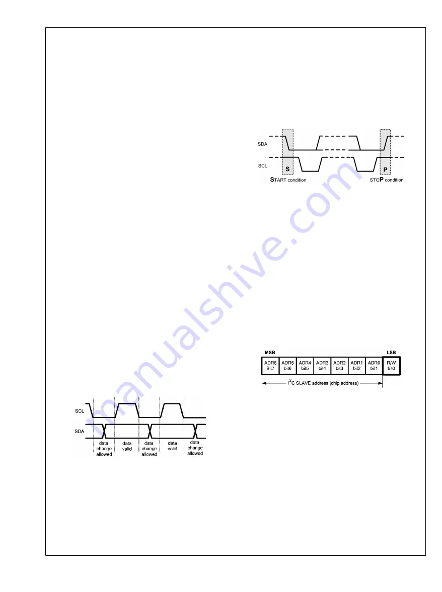
C START AND STOP CONDITIONS
START and STOP conditions classify the beginning and the
end of the I
2
C session. START condition is defined as SDA
signal transitioning from HIGH to LOW while SCL line is
HIGH. STOP condition is defined as the SDA transitioning
from LOW to HIGH while SCL is HIGH. The I
2
C master always
generates START and STOP bits. The I
2
C bus is considered
to be busy after START condition and free after STOP con-
dition. During data transmission, I
2
C master can generate
repeated START conditions. First START and repeated
START conditions are equivalent, function-wise.
30128224
FIGURE 8. I
2
C Start and Stop Conditions
22.5 TRANSFERRING DATA
Every byte put on the SDA line must be eight bits long, with
the most significant bit (MSB) being transferred first. Each
byte of data has to be followed by an acknowledge bit. The
acknowledge related clock pulse is generated by the master.
The transmitter releases the SDA line (HIGH) during the ac-
knowledge clock pulse. The receiver pulls down the SDA line
during the 9
th
clock pulse, signifying an acknowledge. A re-
ceiver which has been addressed must generate an acknowl-
edge after each byte has been received.
After the START condition, the I
2
C master sends a chip ad-
dress. This address is seven bits long followed by an eighth
bit which is a data direction bit (R/W). For the eighth bit, a “0”
indicates a WRITE and a “1” indicates a READ. The second
byte selects the register to which the data will be written. The
third byte contains data to write to the selected register.
30128225
FIGURE 9. I2C Chip Address
www.ti.com
38
LM49360
Summary of Contents for Boomer LM49360
Page 3: ...5 0 LM49360 Overview 301282h8 FIGURE 1 LM49360 Block Diagram www ti com 2 LM49360...
Page 4: ...6 0 Typical Application 30128211 FIGURE 2 Sub PMU System Diagram 3 www ti com LM49360...
Page 5: ...30128216 FIGURE 3 AP PMU System Diagram www ti com 4 LM49360...
Page 16: ...301282h9 FIGURE 4 PMU State Machine 15 www ti com LM49360...
Page 68: ...30128213 FIGURE 20 Internal Clock Network 67 www ti com LM49360...
Page 128: ...40 0 Schematic Diagram 30128220 FIGURE 36 Demo Board Schematic 127 www ti com LM49360...
Page 129: ...30128245 FIGURE 37 Demo Board Schematic www ti com 128 LM49360...
Page 131: ...30128238 FIGURE 40 Inner Layer 2 30128239 FIGURE 41 Inner Layer 3 www ti com 130 LM49360...
Page 132: ...30128240 FIGURE 42 Inner Layer 4 30128241 FIGURE 43 Inner Layer 5 131 www ti com LM49360...
Page 133: ...30128231 FIGURE 44 Bottom Layer 30128242 FIGURE 45 Bottom Silkscreen www ti com 132 LM49360...
Page 136: ...Notes 135 www ti com LM49360...


