4.5 Clock
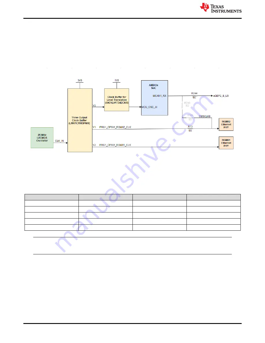
All reference clocks required for the SoC and two Ethernet PHY's are generated from a single three-output clock
buffer (LMK1C1103PWR), which is sourced from a single 25 MHz LVCMOS Oscillator. A single output clock
buffer (SN74LV1TT34DCKR) is used to level translate from 3.3 V to 1.8 V. An optional clock is provided to
RGMII2 Ethernet PHY by the OBSCLK0 output of the SoC by mounting R240 and R185 while isolating R244
and R13.
The reference clock required for XDS110 is generated locally using a 16 MHz crystal.
Figure 4-6. Clock Architecture
Table 4-11. Clock Frequency Table
SI #
Signal Name
Reference
Expected Frequency
1
SOC_CLKIN
U11.4
25.000 MHz
2
SOC_CLKIN_BUFF
R46
25.000 MHz
3
PRG1_CPSW_RGMII1_CLK
R25
25.000 MHz
4
PRG1_CPSW_RGMII2_CLK
R50
25.000 MHz
5
OSC0
Y1.3
16.000 MHz
Note
The 16 MHz clock will only become active after power is supplied to the micro-B USB connector after
insertion of a cable into the micro-B USB port.
Hardware Description
28
AM243x LaunchPad™ Development Kit User's Guide
SPRUJ12B – AUGUST 2021 – REVISED OCTOBER 2022
Copyright © 2022 Texas Instruments Incorporated


