DCLK
Data
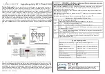
TX controls are
located on this tab
This section controls
power down options
on digital TX chain
Mixing section controls gain, offset,
mixing mode and NCO
This section controls
the TX FIFO
This section controls
auxiliary DACs
RX to TX Loopback
Enable
Trouble Shooting of the EVM Setup
Also the data coming from the TSW3100 is edge aligned while the
AFE722x expect the serial LVDS data to arrive edge centered. Here
the programmable clock delay can be used to delay the edge aligned
clock closer towards the center of the data.
The table below shows clock delays for listed DAC sampling rates
that showed proper operation:.
DAC Sampling Rate
Suitable Clock Delay
130Msps
0ps to 900ps
122.88Msps
0ps to 900ps
100Msps
0ps to 1.2ns
80Msps
0ps to 1.8ns
65Msps
0ps to 2.1ns
40Msps
0ps to 2.1ns
The other portion of the TX setup is located on the
‘
Transmit Control
’
tab which includes register access
for the mixing stage, FIFO, Loopback and power options for the digital TX section. Also the auxiliary DAC
registers are configured on this tab.
9
Trouble Shooting of the EVM Setup
The two main problems engineers face are covered in this chapter. Often times a programming step is
missed leading to faulty or no data either on the RX or TX side. Please refer to AFE722x Setup.pdf in the
support documentation which includes more detailed instructions along with power measurements for
correlation.
The second issue covers unsuccessful data transfer from the TSW3100 to the AFE722x EVM. This most
likely can be traced back to an IP address conflict between the PC and the TSW3100. The following steps
should provide a solution for that problem.
TSW3100 IP Configuration
15
SLOU330
–
December 2011
EVM Description
Copyright
©
2011, Texas Instruments Incorporated


