VEEK-MT2 User Manual
17
www.terasic.com
July 4, 2016
MIPI Decoder
The MIPI camera module output interface is MIPI interface, which can not directly connect to the
Terasic FPGA board; therefore, a MIPI Decoder (TC358748XBG) is added to convert MIPI interface to
a parallel port interface. Decoder users can quickly obtain the image data and process it. MIPI Decoder
can convert MIPI Interface up to 24-bit data. The Camera module used on the D8M can only output 10
bit data, MIPI_PIXEL_D[9:0] the HSMC connector is the camera image output data bus.
FPGA also can read/write MIPI Decoder through a I2C bus (MIPI_I2C_SDA / MIPI_I2C_SCL ; I2C
device address is 0x1C), which is different from the camera module I2C bus. On the VEEK-MT2 board,
MIPI Decoder can output clocks to the MIPI camera and FPGA board. So in the demonstrations, most of
them show how to control IC PLL parameters as well as others. Detailed clock functions are described
in blow.
Clock Tree
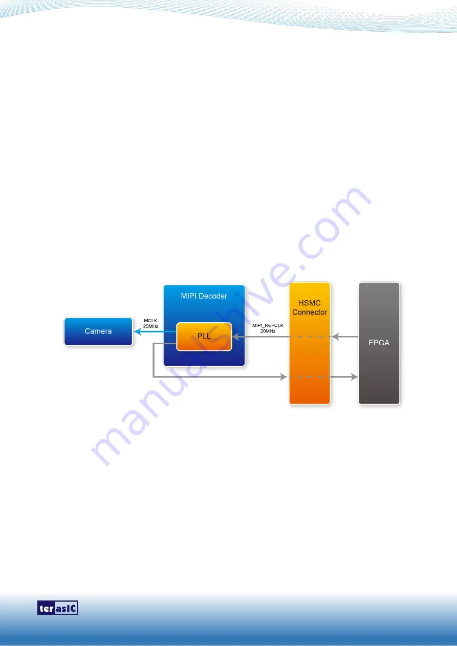
is the VEEK-MT2 board‟s camera clock tree block diagram. MIPI Decoder PLL receives
FPGA Reference Clock (MIPI_REFCLK) and outputs Clock to Camera sensor (MCLK), at the same
time, MIPI Decoder PLL will also output a parallel port clock (MIPI_PIXEL_CLK) and feedback to the
FPGA to deal with parallel data.
Figure 3-8 Block Diagram of the Bus Controller
In the provided demonstrations, MIPI_REFCLK is set to 20MHz, FPGA transmits this clock to the
VEEK-MT2‟s MIPI Decoder PLL through the HSMC connector. No matter how much the camera
resolution is, the MCLK fixed output is 25MHz. According to the output resolution, MIPI_PIXEL_CLK
can be set as 25MHz for 640x480@60fps and 50MHz for 1920x1080@15fps.
For more MIPI Decoder PLL setting details, please refer to TC358746AXBG_748XBG_rev09.pdf
"Chapter 5: Clock and System" or refer to Terasic demonstrations.
Summary of Contents for VEEK-MT2
Page 1: ...1 ...


