background image


VEEK-MT2 User Manual


11


www.terasic.com 
July 4, 2016 


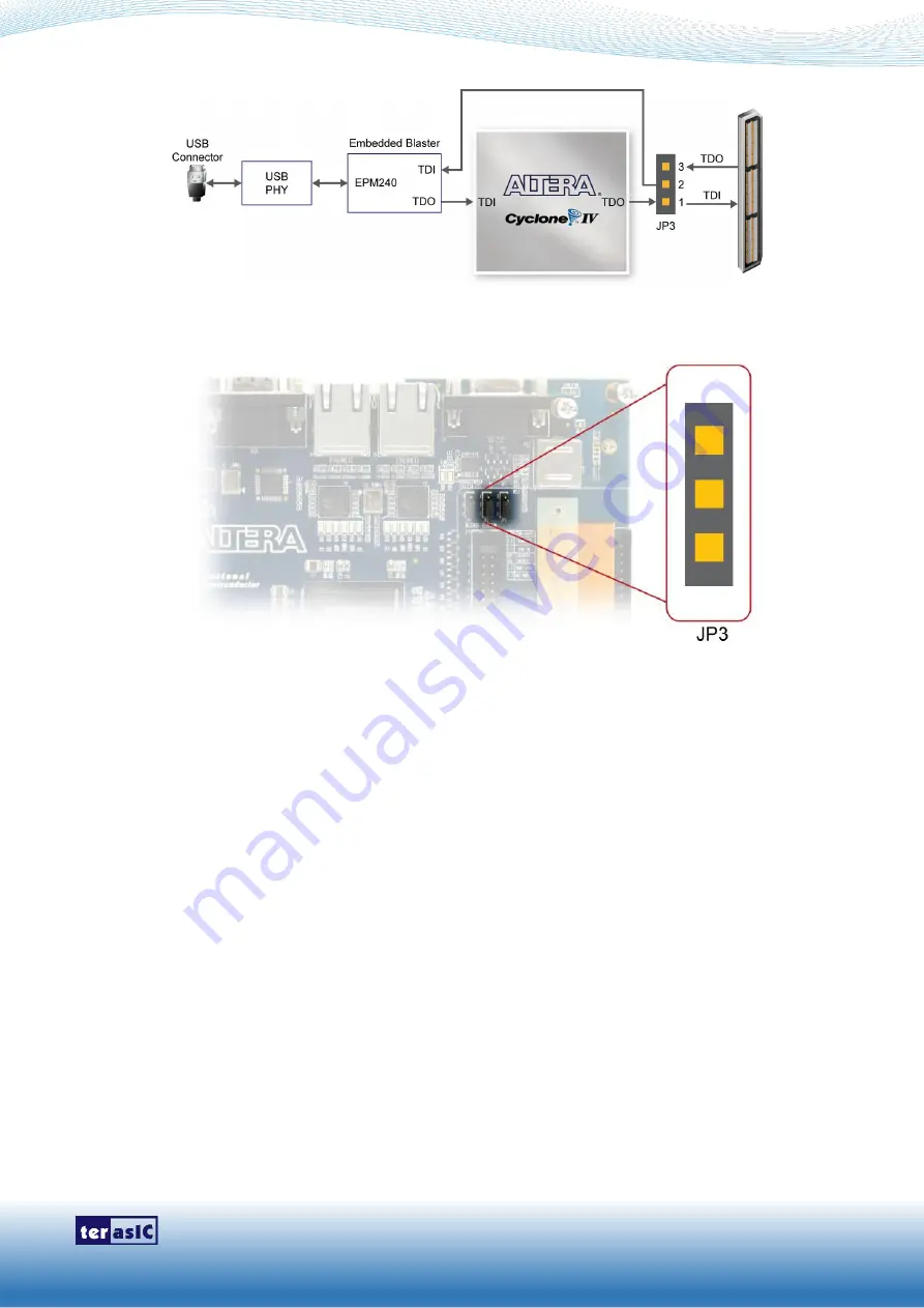
Figure 3-1    JTAG Chain 


Figure 3-2 JTAG Chain Configuration Header 


Configuring the FPGA in JTAG Mode 

Figure  3-3

  illustrates  the  JTAG  configuration  setup.  To  download  a  configuration  bit  stream  into  the 

Cyclone IV E FPGA, perform the following steps: 


Ensure that power is applied to the VEEK-MT2 


Configure  the  JTAG  programming  circuit  by  setting  the  RUN/PROG  slide  switch  (SW19)  to  the 

RUN position (See 

Figure 3-4

) 


Connect the supplied USB cable to the USB-Blaster port on the VEEK-MT2 


The  FPGA  can  now  be  programmed  by  using  the  Quartus  II  Programmer  module  to  select  a 

configuration bit stream file with the .sof filename extension 


Summary of Contents for VEEK-MT2

Page 1: ...1 ...

Page 2: ...1 Configuring the Cyclone IV E FPGA 10 3 2 Bus Controller 13 3 3 Using the 7 LCD Capacitive Touch Screen 14 3 4 Using 8 megapixel Digital Image Sensor 15 3 5 Using the Gyroscope Accelerometer and Magnetometer 19 3 6 Using the Ambient Light Sensor 20 3 7 Using Terasic Multi touch IP 20 Chapter 4 VEEK MT2 Demonstrations 23 4 1 System Requirements 23 4 2 Factory Configuration 23 4 3 Painter Demonstra...

Page 3: ...Demonstration 40 4 9 E Compass Demonstration 43 Chapter 5 Application Selector 48 5 1 Ready to Run SD Card Demos 48 5 2 Running the Application Selector 49 5 3 Application Selector Details 49 5 4 Restoring the Factory Image 52 Chapter 6 Appendix 54 6 1 Revision History 54 6 2 Copyright Statement 54 ...

Page 4: ...light sensor and 3 axis accelerometer make up the rich feature set The VEEK MT2 is preconfigured with an FPGA hardware reference design including several ready to run demonstration applications stored on the provided SD card Software developers can use these reference designs as their platform to quickly architect develop and build complex embedded systems By simply scrolling through the demos of ...

Page 5: ... 4 push buttons o 18 red and 9 green LEDs o Eight 7 segment displays Audio o 24 bit encoder decoder CODEC o 3 5mm line in line out and microphone in jacks Character Display o 16x2 LCD module On board Clocking Circuitry o Three 50MHz oscillator clock inputs o SMA connectors external clock input output SD Card Socket o Provides SPI and 4 bit SD mode for SD Card access Two Gigabit Ethernet Ports o In...

Page 6: ...keyboard TV in Connector o TV decoder NTSC PAL SECAM Remote Control o Infrared receiver module Power o 12V DC input o Switching and step down regulators LM3150MH Capacitive LCD Touch Screen Equipped with an 7 inch Amorphous TFT LCD Thin Film Transistor Liquid Crystal Display module Module composed of LED backlight Support 24 bit parallel RGB interface Converting the X Y coordination of touch point...

Page 7: ...evel calibration ABLC Programmable controls for frame rate mirror and flip cropping and windowing MIPI to Parallel Port Converter Table 1 2 shows the key parameters of the CMOS sensor Note Table 1 2 Key performance parameters of the CMOS sensor Parameter Value Active Pixels 3264Hx2448V Pixel size 1 4umx1 4um Color filter array RGB Bayer pattern ADC resolution 10 bit Pixel dynamic range 68 8dB SNRM...

Page 8: ...agnetometer 3 axis silicon monolithic Hall effect magnetic sensor with magnetic concentrator Wide dynamic measurement range and high resolution with lower current consumption Output data resolution of 14 bit 0 6μT LSB or 16 bit 15μT LSB Full scale measurement range is 4800μT Magnetometer normal operating current 280μA at 8Hz repetition rate Self test function with internal magnetic source to confi...

Page 9: ...tem CD contains technical documents of the VEEK MT2 which includes component datasheets demonstrations schematic and user manual Figure 1 2 VEEK MT2 kit package contents 1 2 Getting Help Here is information of how to get help if you encounter any problem Terasic Technologies 9F No 176 Sec 2 Gongdao 5th Rd East Dist Hsinchu City 30070 Taiwan Tel 886 3 5750 880 Email support terasic com ...

Page 10: ...ecture of the VEEK MT2 including block diagram and components 2 1 Layout and Components The picture of the VEEK MT2 is shown in Figure 2 1 and Figure 2 2 It depicts the layout of the board and indicates the locations of the connectors and key components Figure 2 1 VEEK MT2 PCB and Component Diagram top view ...

Page 11: ...view 2 2 Block Diagram of the VEEK MT2 Figure 2 3 gives the block diagram of the VEEK MT2 board To provide maximum flexibility for the user all connections are made through the Cyclone IV E FPGA device Thus the user can configure the FPGA to implement any system design Figure 2 3 Block Diagram of VEEK MT2 ...

Page 12: ... 2 1 gives the difference between VEEK MT2 and VEEK MT Table 2 1 Difference between VEEK MT2 and VEEK MT Signal Name VEEK MT2 VEEK MT LCD Touch Point 5 Point Touch 2 Point Touchs Camera Module 8 Mega Pixel Auto Focus MIPI Decoder 5 Mega Pixel Motion Sensors Gyroscope Accelerometer Magnetometer Accelerometer ...

Page 13: ...is applied to the board the configuration information will be lost when the power is turned off 2 AS programming In this method called Active Serial programming the configuration bit stream is downloaded into the Altera EPCS64 serial configuration device It provides non volatile storage of the bit stream so that the information is retained even when the power supply to the VEEK MT2 is turned off W...

Page 14: ...ream into the Cyclone IV E FPGA perform the following steps Ensure that power is applied to the VEEK MT2 Configure the JTAG programming circuit by setting the RUN PROG slide switch SW19 to the RUN position See Figure 3 4 Connect the supplied USB cable to the USB Blaster port on the VEEK MT2 The FPGA can now be programmed by using the Quartus II Programmer module to select a configuration bit strea...

Page 15: ... Connect the supplied USB cable to the USB Blaster port on the VEEK MT2 Configure the JTAG programming circuit by setting the RUN PROG slide switch SW19 to the PROG position The EPCS64 chip can now be programmed by using the Quartus II Programmer module to select a configuration bit stream file with the pof filename extension Once the programming operation is finished set the RUN PROG slide switch...

Page 16: ...roller Introduction The bus controller provides level shifting functionality from 2 5V HSMC to 3 3V domains Block Diagram of the Bus Controller Figure 3 6 gives the block diagram of the connection setup from the HSMC connector to the bus controller on the Max II EPM240 to the touch screen module To provide maximum flexibility for the user all connections are established through the HSMC connector ...

Page 17: ...or data along with the data enable and clock signals must act according to the timing specification of the LCD touch panel as shown in Table 3 1 and Table 3 2 Table 3 3 gives the pin assignment information of the LCD touch panel Table 3 1 LCD Horizontal Timing Specifications Item Symbol Typical Value Unit Min Typ Max Horizontal Display Area thd 800 DCLK DCLK Frequency fclk 26 4 33 3 46 8 MHz One H...

Page 18: ...data bus bit 5 2 5V LCD_G6 U26 LCD green data bus bit 6 2 5V LCD_G7 U25 LCD green data bus bit 7 2 5V LCD_HSD U22 Horizontal sync input 2 5V LCD_MODE L24 DE SYNC mode select 2 5V LCD_POWER_CTL M25 LCD power control 2 5V LCD_R0 V28 LCD red data bus bit 0 2 5V LCD_R1 V27 LCD red data bus bit 1 2 5V LCD_R2 U28 LCD red data bus bit 2 2 5V LCD_R3 U27 LCD red data bus bit 3 2 5V LCD_R4 R28 LCD red data ...

Page 19: ...sheet named OV8865 Data Sheet pdf in the VEEK MT2 System CD Figure 3 7 Block Diagram of the Bus Controller Voice Coil Motor VCM There is a Voice Coil Motor VCM driver chip named VCM149C on the MIPI camera module Users can use the same I2C bus I2C device address is 0x18 to modify the DAC value in the VCM driver chip that can allow the VCM to move its lens to the desired position for getting a sharp...

Page 20: ... the demonstrations most of them show how to control IC PLL parameters as well as others Detailed clock functions are described in blow Clock Tree Figure 3 8 is the VEEK MT2 board s camera clock tree block diagram MIPI Decoder PLL receives FPGA Reference Clock MIPI_REFCLK and outputs Clock to Camera sensor MCLK at the same time MIPI Decoder PLL will also output a parallel port clock MIPI_PIXEL_CLK...

Page 21: ...I_PIXEL_D 10 M26 Reserve 2 5V MIPI_PIXEL_D 11 M25 Reserve 2 5V MIPI_PIXEL_D 12 AF27 Reserve 2 5V MIPI_PIXEL_D 13 AE28 Reserve 2 5V MIPI_RESET_n D27 Master Reset signal for MIPI camera and bridge device 2 5V MIPI_PIXEL_CLK J27 Parallel Port Clock signal 2 5V MIPI_PIXEL_HS K26 Parallel Port Horizontal Synchronization signal 2 5V MIPI_PIXEL_VS K25 Parallel Port Vertical Synchronization signal 2 5V MI...

Page 22: ...t the displacement differentially The MPU 9250 s architecture reduces the accelerometers susceptibility to fabrication variations as well as to thermal drift When the device is placed on a flat surface it will measure 0g on the X and Y axes and 1g on the Z axis The accelerometers scale factor is calibrated at the factory and is nominally independent of supply voltage Each sensor has a dedicated si...

Page 23: ...at represents the irradiance measured on each channel This digital output can be input to a microprocessor where illuminance ambient light level in lux is derived using an empirical formula to approximate the human eye response For more detailed information of better using this chip please refer to its datasheet which is available on manufacturer s website or under the datasheet folder of the syst...

Page 24: ... signals in the 2x20 GPIO header respectively When touch activity occurs the control application should check whether the value of oREG_GESTURE matches a pre defined gesture ID defined in Table 3 4 and the relative X Y coordinates can be derived from oREG_X and oREG_Y Figure 3 1 shows the signaltap II waveform of the IP When the oREADY rises it indicates touch activity and the associated informati...

Page 25: ...G_Y3 Output 9 bit Y coordinate of second touch point oREG_X4 Output 10 bit X coordinate of first touch point oREG_Y4 Output 9 bit Y coordinate of second touch point oREG_X5 Output 10 bit X coordinate of first touch point oREG_Y5 Output 9 bit Y coordinate of second touch point oREG_TOUCH_COUNT Output 2 bit touch count Valid value is 0 1 or 2 oREG_GESTURE Output 8 bit gesture ID See Table 3 8 I2C_SC...

Page 26: ...laster driver software You can find instructions in the tutorial Getting Started with Altera s DE2 115 Board tut_initialDE2 115 pdf which is available on the DE2 115 system CD Copy the entire demonstrations folder from the VEEK MT2 system CD to your host computer 4 2 Factory Configuration The VEEK MT2 development kit comes preconfigured with a default utility that boots up on power on and allows u...

Page 27: ...ates operate Figure 4 2 shows the hardware system block diagram of this demonstration For LCD display processing the reference design is developed based on the Altera Video and Image Processing Suite VIP The Frame Reader VIP is used for reading display content from the associated video memory and VIP Video Out is used to display the display content The display content is filled by NIOS II processo...

Page 28: ...stration Source Code Project directory Painter Bit stream used Painter sof Nios II Workspace Painter Software Demonstration Batch File Demo Batch File Folder Painter demo_batch The demo batch file includes the following files Batch File test bat test sh FPGA Configure File Painter sof Nios II Program Painter elf ...

Page 29: ...ted successfully you will see a painter GUI in the LCD Figure 4 3 shows the GUI of the Painter Demo The GUI is classified into three areas Palette Canvas and Gesture Users can select pen color from the color palette and start painting in the Canvas area If gesture is detected the associated gesture symbol is shown in the gesture area To clear canvas content click the Clear button Figure 4 4 shows ...

Page 30: ...images and fills the raw result data into frame buffers in SDRAM The VEEK MT2 will show the image the buffer being displayed points to When users touch the LCD Touch Panel it will proceed to display the next buffered image or last buffered image Figure 4 6 shows the block diagram of this demonstration The Nios II CPU here takes a key role in the demonstration It is responsible of decoding the JPEG...

Page 31: ...de Project directory Picture_Viewer Bit stream used Picture_Viewer sof Nios II Workspace Picture_Viewer Software Demonstration Batch File Demo Batch File Folder Picture_Viewer demo_batch The demo batch file includes the following files Batch File test bat test sh FPGA Configure File Picture_Viewer sof Nios II Program Picture_Viewer elf ...

Page 32: ... next image will be displayed after the delay period 8 You can control the slide show as follows Press Forward to advance Reverse to go back to previous image Play Stop to play the slide or stop it On the top corner you will see the Delay period seconds You can increase or decrease the delay period by touching the or buttons The max delay is 120 seconds the min delay is 1 second and the default de...

Page 33: ...ation Line PAL format and picture in picture mixing with a background layer The video stream is output in high resolution 800 480 LCD touch panel The example design demonstrates a framework for rapid development of video and image processing systems using the parameterizable MegaCore functions that are available in the Video and Image Processing Suite Available functions are listed in Table 4 1 Th...

Page 34: ...rmats to progressive video format using a motion adaptive deinterlacing algorithm Also supports bob and weave algorithms Test Pattern Generator Generates a video stream that contains still color bars for use as a test pattern Clipper II Provides a way to clip video streams and can be configured at compile time or at run time Color Plane Sequencer Changes how color plane samples are transmitted acr...

Page 35: ...run time is also provided The video system is implemented using the QSYS system level design tool This abstracted design tool provides an easy path to system integration of the video processing data path with a NTSC or PAL video input VGA output Nios II processor for configuration and control The Video and Image Processing Suite MegaCore functions have common open Avalon ST data interfaces and Ava...

Page 36: ...r both LCD and CRT type of monitors should work Load the bit stream into FPGA note Run the Nios II and choose VIP Software as the workspace Click on the Run button note Connect a DVD player s composite video output yellow plug to the Video IN RCA jack J12 of the VEEK MT2 The DVD player has to be configured to provide NTSC output or PAL output Press and drag the video frame box will result in scali...

Page 37: ...etup for the VIP demonstration 4 6 Camera Application This demonstration shows a digital camera reference design using the 8 Megapixel CMOS sensor and LCD modules on the VEEK MT2 The CMOS sensor module sends the raw image data to FPGA on the DE2 115 board the FPGA on the board handles image processing part and converts the data to RGB format to display on the LCD module ...

Page 38: ... Block diagram of the digital camera design MIPI_BRIDGE_CAMERA_Config the MIPI BRIDGE I2C and Camera I2C setting controller such as set to output 800X480 60Hz timing It mainly writes I2C corresponding parameters to MIPI BRIDGE IC register and Camera Sensor IC register respectively through their own I2C buses MIPI_I2C bus is used to write MIPI BRIDGE I2C I2C Slave Address 0x1c CAMERA_I2C bus is use...

Page 39: ...15 board Load the bit stream into FPGA by executing the batch file test bat under Camera demo_batch folder The system enters the FREE RUN mode automatically See Figure 4 12 LED0 1 light up stand the settings of MIPI BRIDGE I2C and Camera I2C are completed LED7 9 blink in 1Hz stand MIPI PIXEL CLOCK MIPI REF CLOCK and MT2 PIXEL CLOCK are generated correctly HEX1 0 decimal number 60 stands Camera cap...

Page 40: ...ful LED 7 Blink in 1Hz MIPI PIXEL CLOCK 50M LED 8 Blink in 1Hz MIPI REF CLOCK 20M LED 9 Blink in 1HZ LCD PIXEL CLOCK 33M KEY 0 SYSTEM RESET ZOOM IN Gesture Area Focus Mode ZOOM Out Gesture Whole Area Focus Mode HEX 1 0 Frames Per Second FPS Figure 4 12 Screen shot of the VEEK MT2 camera demonstration Figure 4 13 Area Focus Mode of the VEEK MT2 camera demonstration Note Executing the test bat under...

Page 41: ...in the FPGA These functions include clipping chroma resampling motion adaptive deinterlacing color space conversion picture in picture mixing and polyphase scaling The input and output video interfaces on the VEEK MT2 are configured and initialized by software running on a Nios II processor Nios II software demonstrates how to control the clocked video input clocked video output and mixer function...

Page 42: ...Diagram Key Components Demonstration Source Code Project directory VIP_Camera Bit stream used VIP_Camera sof Nios II Workspace VIP_Camera Software Demonstration Batch File Demo Batch File Folder VIP_Camera demo_batch The demo batch file includes the following files Batch File test bat test sh FPGA Configure File VIP_Camera sof Nios II Program VIP_Camera elf ...

Page 43: ...mmunicate with MPU9250 to retrieve the gravity information and another is used to communicate with the APDS 9300 Miniature Ambient Light Photo Sensor The demonstration using the gravity information retrieved from the MPU9250 to implement a bubble level on the LCD panel When tilting the VEEK MT2 the NIOS II program reads the acceleration of gravity from the MPU9250 Based on the gravity information ...

Page 44: ...r cpp The MPU9250 class implemented in the MPU9250 cpp h is used to retrieve accelerometer information from the MPU9250 The member function initialize of the MPU9250 class should be called first before calling any other member function In this demonstration the member function getMotion9 is called to get the gravity value of X Y Z The light_sensor cpp h includes the library which allows it to comm...

Page 45: ...test bat to configure FPGA and launch the NIOS II program Note Tilt the VEEK MT2 to all directions and you will find that the angle of the g sensor and value of light sensor will change When turning the board from 80º to 10º and from 10º to 80º in Y axis or from 10ºto 80º and from 80º to 10º in Y axis the image will invert Figure 4 17 shows the demonstration in action Figure 4 17 Digital Accelerom...

Page 46: ... left area show the gravity information measured by accelerometer in the MPU9250 Also a bubble level is shown on the LCD The center of LCD panel shows the e compass The north direction and magnetic field information are shown on the LCD panel The Calibration button is used to start the calibration process for the e compass Figure 4 18 Graphic Interface of e compass demonstration Figure 4 19 shows ...

Page 47: ...p ID of APDS 9300 The Function Light_Get_ADCData0 and Light_Get_ADCData1 are designed to get the two ADC values in APDS 9300 The section introduces the method to calculate the heading angle based on the values measured by accelerometer and magnetometer in this demonstration If the compass is on a flat surface then heading angle can be calculated with the following formula arctan Xh Yh where Xh and...

Page 48: ...arth s magnetic field locally and are related to scaling offset errors In other words to get the correct magnetometer data you should calibrate it first In this demonstration we corrected the magnetic field with the following formula Xcalibrated X Xoffset Ycalibrated Y Yoffset Zcalibrated Z Zoffset where Xoffset Yoffset and Zoffset area the average value of X Y Z magnetic field defined as Xoffset ...

Page 49: ...ote The E Compass will be displayed on the LCD panel Touch the Calibration button to start the calibration process When the button is touched the LCD content will be changed as shown in Figure 4 21 Rotate VEEK MT2 in X Y Z axis individually Touch the Finished button when rotation is done When the Finished button is touched the LCD content is changed as shown in Figure 4 22 The minimal maximal and ...

Page 50: ...EK MT2 User Manual 47 www terasic com July 4 2016 Figure 4 21 Hint for rotate VEEK MT2 Figure 4 22 Magnetic Calibration Information Note Execute E_Compass demo_batch test bat to download sof and elf files ...

Page 51: ...n SD card demos in your SD card root directory as well as in the System CD under Factory_Recovery Application_Selector folder Figure 5 1 shows the photograph of the application selector main interface Figure 5 1 Application selector main interface Also you can easily convert your own applications to be loadable by the application selector For more information see Creating Your Own Loadable Applica...

Page 52: ...Card The Application Selector uses an SD card for storing applications The SD card must be formatted with the FAT 16 file system and can be any capacity up to 4GB Long file names are supported The Nios II CPU access the SD card through an SD card SPI controller Application Files Each loadable application consists of two binary files all stored on the SD card The first binary file represents the so...

Page 53: ...offset 0x0 EPCS Device EPCS is used to store both the binary file of the Application Selector both hardware and software image itself as well as hardware binary files of applications which are being loaded The Application Selector binary file is permanently stored in EPCS device at offset 0x0 Hardware binary files for the applications being loaded get written to EPCS at load time to an offset 0x40...

Page 54: ...ike this Application_Selector Name of Application elf_name _SW bin sof_name _HW bin Place the SD card in the VEEK MT2 and switch on the power The Application Selector will start up and you will now see your application appear as one of the selections Note 1 You may not need a CFI Flash controller when your design does not contain a Nios II processor or you store your software code within the on ch...

Page 55: ...Selector_HW bin From the command shell navigate to where your ELF file is located and create your software bin image using the following command commands listed below Convert Selector elf into Selector_SW flash elf2flash epcs after Selector_HW flash input Selector elf output Selector_SW flash Convert Selector_SW flash into Selector_SW bin nios2 elf objcopy I srec O binary Selector_SW flash Selecto...

Page 56: ...ic com July 4 2016 Note You can also use Selector_batch to generate selector bin and restore the original binary file by executing the Selector bat under the Factory_Recovery Selector_batch folder Figure 5 2 Programming Flash settings ...

Page 57: ...er Manual 54 www terasic com July 4 2016 Chapter 6 Appendix 6 1 Revision History Version Change Log V1 0 Initial Version Preliminary 6 2 Copyright Statement Copyright 2016 Terasic Technologies All rights reserved ...

Page 58: ...Mouser Electronics Authorized Distributor Click to View Pricing Inventory Delivery Lifecycle Information Terasic P0471 P0471 EDU ...

Reviews: