background image

M805-00

Glossary Of Terms

A1

Copyright TEL

30/09/96

Appendix A

Glossary Of Terms

Absolute Delay

The time a signal is delayed, measured from when it
leaves its source to when it reaches its destination.

ACL-II+ Card

One of two additional cards (the other is a PCL-830
card) fitted into a standard IBM

1

 compatible 386 (or

better) computer to enable it to operate as a System
Controller.  The ACL-II+ card provides the RS-485
serial communication between the computer and
ASP cards.

AIM

Audio Inversion Module (T805-01).  The AIM is
used when Quasi-Synchronous transmitters are
remotely located and linked to the base site via a
land line. Audio in the 67Hz to 2.55kHz band is
inverted and shifted around a carrier so that it can be
sent down a 300Hz to 3kHz channel.  The methods
employed also offer immunity to line polarity
reversals and amplitude variations of the land line.

Amplitude Response

The variation in amplitude of a signal as its fre-
quency is changed.

ARM

Audio Recovery Module (T805-01).  A complement
to the AIM.

ASP Card

Audio Signal Processing card.  The hardware
description for the cards used in the Quasi-Synchro-
nous system.  An ASP card can be a TSGM, LEM,
AIM or ARM depending on the software used.

Breakout Mode

The mode that a LEM/transmitter combination may
be put into if it is required to work outside the
Quasi-Synchronous system.  The audio information
transmitted by this combination will be different to
that which is being transmitted by the Quasi-Syn-
chronous system.

Card ID

A number in the range 0-255 which is used to
uniquely identify a card.  An LEM may be in the
range 0-222 while a TSGM has the address in the
range 223-238.

Controlling System

The (host) system to which the Quasi-Synchronous
system is connected.

1.

IBM is a registered trade-mark of International Business Machines Ltd.

1

Summary of Contents for T805

Page 1: ...ovide additional information The List of Effective Pages and Tables Of Contents have also been updated to reflect these changes Contents You can update your M805 00 101 to revision 102 status by sub stituting or adding these Revision Package pages as instructed in the following table Section Revision Package Page Numbers Pages To Replace Add In Sequence After Page TOC LEP 1 to 8 1 to 8 1 1 5 to 1 ...

Page 2: ...it Internal Part Number IPN R805 00 102 when ordering 14 1 14 1 1 to 14 1 2 14 1 1 to 14 1 2 14 2 14 2 1 to 14 2 2 14 2 1 to 14 2 2 14 3 14 3 1 to 14 3 2 14 3 13 to 14 3 22 14 3 1 to 14 3 2 14 3 12 14 4 14 4 9 to 14 4 10 14 4 9 to 14 4 10 14 5 14 5 1 to 14 5 6 14 4 14 App A A1 to A4 A1 to A4 Section Revision Package Page Numbers Pages To Replace Add In Sequence After Page ...

Page 3: ...M805 00 1 Copyright TEL 30 09 96 T805 Quasi Synchronous Transmission System Service Manual Issue 102 October 1996 M805 00 102 ...

Page 4: ...many Tait Mobilfunk GmbH Willstätterstraße 50 D 90449 Nürnberg 60 Germany Phone 49 911 96 746 0 Fax 49 911 96 746 79 Hong Kong Tait Mobile Radio HK Ltd Room 703A New East Ocean Centre 9 Science Museum Road Tsim Sha Tsui East Hong Kong Phone 852 2369 3040 Fax 852 2369 3009 New Zealand Tait Communications Ltd Unit 4 75 Blenheim Road P O Box 1185 Christchurch Phone 64 3 348 3301 Fax 64 3 343 0558 Sin...

Page 5: ...e List of Effective Pages and a new list containing any new revised pages and their publica tion dates will be sent with each revision package Any portion of text that has been changed is marked by a verti cal line as shown at left in the outer margin of the page Where the removal of an entire paragraph means there is no text left to mark an arrow as shown at left will appear in the outer mar gin ...

Page 6: ...ent And Manuals In the interests of improving performance reliability or servicing Tait Electronics Ltd reserve the right to update their equipment and or manuals without prior notice Copyright All information contained in this manual is the property of Tait Electronics Ltd All rights are reserved This manual may not in whole or part be copied photocopied reproduced translated stored or reduced to...

Page 7: ... Information 2 System Description 3 Circuit Operation 4 ASP Card Operation 5 Quasi Synchronous Operation With Audio Distribution Net works 6 Introduction To Servicing 7 Initial Programming Adjustment 8 Functional Tests 9 Fault Finding 10 T805 04 Backplane 11 T805 06 1U Rack 12 T805 System Controller 13 Commissioning Tests 14 PCB Information Appendix A Glossary Of Terms Appendix B Decimal Hex Binar...

Page 8: ... 2 5 30 04 95 2 6 30 04 95 3 1 30 04 95 3 2 30 04 95 3 3 30 04 95 3 4 30 04 95 3 5 30 04 95 3 6 30 04 95 3 7 30 04 95 3 8 30 04 95 3 9 30 04 95 3 10 30 04 95 3 11 30 04 95 3 12 30 04 95 3 13 30 04 95 3 14 30 04 95 3 15 30 04 95 fold out 3 16 blank fold out 4 1 30 09 96 4 2 blank 4 3 30 09 96 4 4 30 09 96 4 5 30 09 96 4 6 30 09 96 4 7 30 09 96 4 8 30 09 96 4 9 30 09 96 4 10 30 09 96 5 1 30 04 95 5 ...

Page 9: ... 6 30 09 96 10 7 30 04 95 10 8 30 04 95 10 9 30 04 95 10 10 30 04 95 10 11 30 09 96 10 12 30 04 95 10 13 30 09 96 10 14 30 04 95 10 15 30 04 95 10 16 30 09 96 10 17 30 09 96 10 18 30 09 96 10 19 30 04 95 10 20 blank 11 1 30 04 95 11 2 blank 11 3 30 04 95 11 4 30 04 95 11 5 30 04 95 11 6 blank 12 1 30 04 95 12 2 blank 12 3 30 04 95 12 4 blank 13 1 30 04 95 13 2 blank 13 3 30 04 95 13 4 30 09 96 13 ...

Page 10: ...old out 14 3 21 30 09 96 fold out 14 3 22 30 09 96 fold out 14 4 1 30 04 95 14 4 2 30 04 95 14 4 3 30 04 95 14 4 4 blank 14 4 5 30 04 95 14 4 6 30 04 95 14 4 7 30 04 95 14 4 8 blank 14 4 9 30 09 96 14 4 10 30 09 96 14 4 11 30 04 95 14 4 12 30 04 95 14 4 13 30 04 95 fold out 14 4 14 blank fold out 14 5 1 30 09 96 14 5 2 30 09 96 14 5 3 blank 14 5 4 30 09 96 14 5 5 30 09 96 fold out 14 5 6 30 09 96 ...

Page 11: ...plus back up Audio Interfaces Inputs Quasi Synchronous Audio 600Ω balanced via rack From RIC External CTCSS Optional 47kΩ balanced Outputs LF Training Signal CTCSS 600Ω balanced via rack HF Training Signal Q S Audio 600Ω balanced via rack Audio Bandwidth 67Hz to 3kHz or 67Hz to 2550Hz depending on configuration Signal To Noise Ratio 50dB Distortion 1 Audio Input And Output Levels 10dBm nominal int...

Page 12: ... Bandwidth 300Hz to 3kHz or 67Hz to 3kHz depending on input or output Signal To Noise Ratio 50dB Distortion 1 Input And Output Levels 10dBm nominal into a balanced load Maximum Audio Input And Output Levels 0dBm into a 600Ω balanced load Digital Inputs GPS sample training tone ICCS breakout Communication With Q S Controller RS 485 1 2 6 Audio Interface Card AIM Audio Interfaces Input Audio In 600Ω...

Page 13: ...Card ARM Audio Interfaces Input Audio In 600Ω balanced via rack Outputs Audio Out Optional Keytone 600Ω balanced CTCSS 600Ω balanced Audio Bandwidth Input Speech CTCSS Control Signals 350Hz to 3kHz Outputs Audio Out 67Hz to 2550Hz CTCSS 67Hz to 300Hz Keytone Optional 2970Hz Signal To Noise Ratio 50dB Distortion 1 Input And Output Levels 10dBm nominal into a balanced load Maximum Audio Input And Ou...

Page 14: ...5 06 1U Rack Maximum Number Of ASP Cards Per Rack 1 Type of ASP Cards To Be Fitted T805 01 AIM T805 01 ARM Power Supply2 13 8V DC capable of supplying 1A Input Signals Telecom 4W3 monitor receiver audio Output Signals Telecom 4W transmit audio transmit CTCSS low frequency training tones Termination Types Audio terminal blocks Telecom via Line Barrier Unit3 1 2 10 AIM ARM Communications Link Type O...

Page 15: ...aliser Module LEM 4 6 4 3 T805 01 Audio Inversion And Recovery Modules AIM ARM 4 7 4 3 1 T805 01 Audio Inversion Module AIM 4 7 4 3 1 1 Local Mode 4 8 4 3 1 2 Remote Mode 4 8 4 3 2 T805 01 Audio Recovery Module ARM 4 9 4 3 2 1 Remote Mode 4 9 4 3 2 2 Local Mode 4 10 Figure Title Page 4 1 TSGM Block Diagram 4 3 4 2 LEM Block Diagram 4 6 4 3 AIM Block Diagram 4 7 4 4 Example Of Signals Fed Into An A...

Page 16: ...4 2 ASP Card Operation M805 00 30 04 95 Copyright TEL ...

Page 17: ...red by the LEMs during the training process When the system is operating normally in pass mode i e not in the training mode the TSGM passes the normal speech audio 0 3200Hz for software v2 09 v2 10 v2 11 0 2550Hz for v2 12 v2 13 from the appropriate input depending on system configu ration to output 1 and after that to all the LEMs The signal path followed will depend on the system type to which t...

Page 18: ...g programmed via DIP switches on the board Alternatively the CTCSS may be exter nally supplied but must be passed into the TSGM via input 2 so that it still exits from audio output 2 Note 3 For TSGM software versions 2 12 and later internal CTCSS is generated only when the ICCS input is at logic 1 and is stopped when the ICCS input becomes logic 0 Versions 2 12 and later support reverse phase burs...

Page 19: ...O is also disabled to prevent inter ference Because the failed TSGM is unable to answer polls the System Controller will then instruct the other TSGM if fitted to connect its audio lines and thus become the system TSGM For more information on control of the TSGM by the System Controller refer to the Sys tem Controller manual Network Number TSGM ID Numbers Decimal 1 2 3 4 5 6 7 8 223 224 225 226 22...

Page 20: ... input of each LEM Only the LEM being trained will respond to it The audio inputs and outputs of the LEM may be configured in various ways the sys tem configuration defining how these are selected refer to Figure 4 2 and Section 5 Under normal operating conditions the LEMs operate in the Quasi Synchronous equalised mode but any LEM may be removed from Quasi Synchronous operation to operate indepen...

Page 21: ... is proc essed to adapt the signal for a 300Hz to 3kHz frequency bandwidth and so minimises any possible effects that the link may introduce It is then passed into the line connect ing to the appropriate site At this site the signal is passed into an ARM where it is recovered to restore the original signal If required the signals are then separated audio and CTCSS and fed into the transmitter Cont...

Page 22: ...lling tones are shifted from the 67 2550Hz band to a 350 2833Hz band by being mixed with an internally generated 2900Hz carrier base band shifting This allows the equalised audio signal which includes CTCSS to be sent along a land line It also offers immunity to total audio cancellation due to line reversals The baseband shifted audio CTCSS signal and 2900Hz carrier are transmitted down the link t...

Page 23: ...900Hz key tone at the input places the ARM in the recovery mode and it uses this 2900Hz carrier to recover the original audio by demodula tion The inverted speech CTCSS and signalling if used is shifted down to the nominal bands of 67 300Hz for CTCSS and 300 2550Hz for the speech signalling DIP switches D5 and D6 are used to configure the outputs D5 determines whether or not a 2970Hz key tone is p...

Page 24: ...Figure 4 7 ARM Operation When In Remote Recovery Mode 4 3 2 2 Local Mode In this mode the ARM is in the recovery mode permanently Recovery process applied Amplitude Frequency Hz 67 2550 Audio CTCSS 350 2833 2900 Amplitude Inverted audio CTCSS Frequency Hz 1 ...

Page 25: ...output of the RIC is then passed into its corre sponding LEM Because of limitations in PCM technology the RIC s frequency response is limited to the 300Hz to 3kHz band and so CTCSS or training signals below 300Hz cannot be passed to the LEMs via this path The CTCSS is either generated in the TSGM itself or fed into it from an external source The TSGM s LF output is fed directly into all the LEMs i...

Page 26: ...al is split into two bands 300Hz to 3kHz HF training audio and 45 300Hz LF training audio The HF training audio is passed into the ADC 1 system along the same path as normal speech audio while the LF training audio follows the same path as the CTCSS signal They are summed in the LEM as for normal operation and then passed out to the transmitter for the training process Training is carried out usin...

Page 27: ...vered in this section Section Title Page 7 1 T805 ASP Cards 7 3 7 1 1 Introduction 7 3 7 1 2 DIP Switch Settings 7 3 7 1 3 TSGM 7 8 7 1 3 1 DIP Switch Settings 7 8 7 1 3 2 Audio Links 7 8 7 1 3 3 Line Levels 7 9 7 1 4 LEM 7 10 7 1 4 1 DIP Switch Settings 7 10 7 1 4 2 Audio Links 7 10 7 1 4 3 Line Levels 7 10 7 1 5 AIM 7 11 7 1 5 1 DIP Switch Settings 7 11 7 1 5 2 Audio Links 7 11 7 1 5 3 Line Leve...

Page 28: ...5 02 ASP card LEM 7 4 7 4 DIP switch settings for switches D3 D7 SW301 for a T805 03 ASP card TSGM 7 4 7 5 DIP switch settings for switches D8 D15 SW302 if the ASP card is defined as an LEM These are used to define the address of the card 1 222 Refer to Appendix B for a com plete table of settings 7 5 7 6 DIP switch settings for TSGM addresses when the ASP card is defined as a TSGM 7 5 7 7 DIP swi...

Page 29: ...cedure assumes the T805 ASP card is fitted in a T805 04 backplane or a T805 06 1U rack A T1560 05 rack extension card is recom mended for ease of potentiometer adjustment 7 1 2 DIP Switch Settings The 16 DIP switches D0 D7 of SW301 D8 D15 of SW302 on the ASP card uniquely define what type of card it is and the various operating parameters it needs to operate correctly These operating parameters ar...

Page 30: ...e OFF position the bit value is a logic 1 D3 0 1 local remote defines whether card is remotely located or not D4 not used D5 0 1 keytone required keytone not required defines if the 2970Hz keytone is mixed in with the audio output O P 1 of an ARM D6 0 1 CTCSS in O P 1 CTCSS in O P 2 applies to the ARM only defines if the LF audio is present in the same output as the HF audio O P 1 or is fed to a s...

Page 31: ...when the ASP card is defined as a TSGM LEM Address D8 D15 SW302 D8 D9 D10 D11 D12 D13 D14 D15 1 2 3 4 219 220 221 222 1 0 1 0 1 0 1 0 0 1 1 0 1 0 0 1 0 0 0 1 0 1 1 1 0 0 0 0 1 1 1 1 0 0 0 0 1 1 1 1 0 0 0 0 0 0 0 0 0 0 0 0 1 1 1 1 0 0 0 0 1 1 1 1 Network TSGM Address D3 D6 Of SW302 D3 D4 D5 D6 1 1 223 224 0 1 0 0 0 0 0 0 2 2 225 226 0 1 1 1 0 0 0 0 3 3 227 228 0 1 0 0 1 1 0 0 4 4 229 230 0 1 1 1 1 ...

Page 32: ...151 4 156 7 162 2 167 9 173 8 179 9 186 2 192 8 203 5 210 7 218 1 225 7 233 6 241 8 250 3 1 0 1 0 1 0 1 0 1 0 1 0 1 0 1 0 1 0 1 0 1 0 1 0 1 0 1 0 1 0 1 0 1 0 1 1 0 0 1 1 0 0 1 1 0 0 1 1 0 0 1 1 0 0 1 1 0 0 1 1 0 0 1 1 0 0 0 0 0 1 1 1 1 0 0 0 0 1 1 1 1 0 0 0 0 1 1 1 1 0 0 0 0 1 1 1 1 0 0 0 0 0 0 0 0 0 1 1 1 1 1 1 1 1 0 0 0 0 0 0 0 0 1 1 1 1 1 1 1 1 0 0 0 0 0 0 0 0 0 0 0 0 0 0 0 0 0 1 1 1 1 1 1 1 1 ...

Page 33: ...186 2 192 8 203 5 210 7 218 1 225 7 233 6 241 8 250 3 259 1 1 0 1 0 1 0 1 0 1 0 1 0 1 0 1 0 1 0 1 0 1 0 1 0 1 0 1 0 1 0 1 0 1 0 1 0 1 0 1 0 1 1 0 0 1 1 0 0 1 1 0 0 1 1 0 0 1 1 0 0 1 1 0 0 1 1 0 0 1 1 0 0 1 1 0 0 1 1 0 0 0 1 1 1 1 0 0 0 0 1 1 1 1 0 0 0 0 1 1 1 1 0 0 0 0 1 1 1 1 0 0 0 0 1 1 1 1 0 0 0 0 0 0 0 1 1 1 1 1 1 1 1 0 0 0 0 0 0 0 0 1 1 1 1 1 1 1 1 0 0 0 0 0 0 0 0 0 0 0 0 0 0 0 0 0 0 0 0 0 0 ...

Page 34: ...r CTCSS requirements Not relevant to card setting Note Depending on the type of switch used if a switch is pushed down in the position labelled OFF it is at logic 1 or if the switch is pushed towards the LED indicators on the ASP card to the OFF position the bit value is a logic 1 Table 7 9 DIP switch settings for a TSGM 7 1 3 2 Audio Links Short A B 47kΩ on link 3 Refer to Figure 7 1 Figure 7 1 J...

Page 35: ...his sets the maximum input level into the A D converter Monitor the balanced signal at O P 1 on the backplane with an earth isolated audio voltmeter and adjust RV202 for an output level of 10dBm the 600Ω termi nation is on the backplane If internal CTCSS if being used enable CTCSS and set the frequency according to the DIP switch settings in Table 7 7 or Table 7 8 Monitor the balanced signal at O ...

Page 36: ...e OFF position the bit value is a logic 1 Table 7 10 DIP switch settings for an LEM 7 1 4 2 Audio Links Refer to Figure 7 1 ADC 1 system link B C of link 3 600Ω input impedance ADC 2 system link A B of link 3 47kΩ input impedance 7 1 4 3 Line Levels Connect the test equipment as shown in Figure 7 2 Plug the ASP card into the T1560 05 rack extension card and insert it into the appropriate position ...

Page 37: ...IC211 and adjust RV203 to obtain a level of 0dBm This sets the maximum input level into the A D converter 7 1 5 AIM 7 1 5 1 DIP Switch Settings The following are the settings for switches D0 D15 SW301 SW302 if the ASP card is defined as an AIM SW301 SW302 Refer to Table 7 2 for local remote setting Not relevant to card setting Note Depending on the type of switch used if a switch is pushed down in...

Page 38: ...ckplane with an earth isolated audio voltmeter and adjust RV202 for an output level of 10dBm into 600Ω 7 1 6 ARM 7 1 6 1 DIP Switch Settings The following are the settings for switches D0 D15 SW301 SW302 if the ASP card is defined as an ARM SW301 SW302 Refer to Table 7 2 for local remote setting Refer to Table 7 2 for keytone on off switch Refer to Table 7 2 for CTCSS output selection Not relevant...

Page 39: ...and insert it into the appropriate position in the rack Inject a balanced earth isolated 1kHz signal at a level of 10dBm 600Ω into I P 1 of the appropriate port on the T805 04 backplane Monitor pin 24 of IC210 and adjust RV201 to obtain a level of 0dBm This sets the maximum input level into the A D converter Monitor the balanced signal at O P 1 on the backplane with an earth isolated audio voltmet...

Page 40: ...on To properly train the system the CTCSS input into all the transmitters of the Quasi Synchronous system must be connected even if CTCSS is not being used Inject a balanced 1kHz tone at a level of 12dBm into the audio input of the trans mitter Adjust the transmitter modulation sensitivity so that a modulation level of 60 of maximum system deviation is achieved Remove the 1kHz tone Inject a 150Hz ...

Page 41: ...kHz de emphasised frequency response all high pass filtering should be bypassed Refer to the appropriate service manual for more informa tion Inject an on channel RF signal at a level of 47dBm into the monitor receiver Adjust the signal generator for a 1kHz audio signal deviated to 60 of maxi mum system deviation Adjust the line output level to obtain 10dBm into a 600Ω balanced termination ...

Page 42: ...iers is suitable for direct connection to speech band circuits or relevant branch systems for speech band circuits It may be connected to 4W Private Speech Band circuits It must be used only in conjunction with the protection barrier s specified in the instructions for use The T805 is also suitable for point to point circuits The T805 is BABT approved for use only with the CYFAS 88 0507 Line Barri...

Page 43: ...cuit ii Cable or wiring complying with a code of practice for the installation of equipment covered by Section 9 of BS6328 or such other requirements as may be applicable Figure 7 3 shows the levels that should be presented to the Telecom lines if the system is correctly aligned and a balanced test tone of 1kHz at 10dBm is injected into input 1 of the TSGM Note To key the appropriate transmitter i...

Page 44: ...7 18 Initial Programming Adjustment M805 00 30 09 96 Copyright TEL ...

Page 45: ... ASP card has success fully powered up The TEST MODE TSGM LEM and ARM LEDs should light up unless oth erwise indicated The operation of the WDR LED is random in this test mode and should be ignored 8 2 2 2 Analogue Audio Circuitry In this test the electronic relays are in their normal energised state allowing audio to be passed A signal is fed into the main input of each audio interface circuit AI...

Page 46: ... and verify that only the 1kHz signal is present at a level of 10dBm into a 600Ω load Inject a balanced earth isolated 1kHz signal at a level of 10dBm into input 2 600Ω terminations on test lead Monitor the level at TP31 or pin 26 of AIC 2 IC211 and adjust RV203 for a level of 0dBm 2 2V p p Monitor the balanced signal at output 2 or TP26 TP27 when output 2 is termi nated into a 600Ω load Adjust RV...

Page 47: ...p resistor to the DIGOUT line pin 8A of connector PL 1 and connect to 5V Verify that it is at logic 0 0V The DIGOUT LED should also be lit Remove the short on LINK 1 The DIGOUT LED should flash at a rate of approximately 500ms Replace the short on LINK 1 8 2 2 6 RAM Test During test mode 1 the DSP IC is writing AA to each location in the RAM and reading it back to check correct read write operatio...

Page 48: ...ushed towards the LED indicators on the ASP card to the OFF position the bit value is a logic 1 Table 8 2 DIP switch settings for placing the ASP card in test mode 2 8 2 3 2 Audio Interface Circuit In this test the relays are de energised preventing audio output from the AICs reaching the output connector A signal is fed into the main input of each audio interface circuit AIC digitised and passed ...

Page 49: ...ut 2 connector or TP26 TP27 8 2 3 3 Serial Communications Transmitter In this test the RS 485 transmitter is disabled verified by the RS 485 LED being extin guished and the receive mode enabled If the ASP card is sent the ASCII code for the symbols AB the LEM LED will light up for 300ms every time it receives a correctly structured signal Connect the backplane to a computer fitted with RS 485 seri...

Page 50: ...tch used if a switch is pushed down in the position labelled OFF it is at logic 1 or if the switch is pushed towards the LED indicators on the ASP card to the OFF position the bit value is a logic 1 Table 8 3 DIP switch settings for testing the functionality of the DIP switches Connect a 10kΩ pull up resistor to the DIGOUT line pin 8A of connector PL 1 and connect to 5V Verify that it is at logic ...

Page 51: ...ed down in the position labelled OFF it is at logic 1 or if the switch is pushed towards the LED indicators on the ASP card to the OFF position the bit value is a logic 1 Table 8 4 DIP switch settings for placing the ASP card in test mode 3 8 2 4 2 Audio Interface Circuit In this test the electronic relays are in their normal energised state allowing audio out put to be passed to the connector A s...

Page 52: ...4 3 Watchdog Timer The short on LINK 1 should be removed when entering test mode 3 If all the LEDs except the AIM LED flash refer to Section 9 4 for fault finding information 8 2 4 4 Digital I O The following test and the corresponding test in Section 8 2 3 5 verify that all the DIP switches are functioning correctly Set the DIP switches SW301 SW302 as shown in Table 8 5 Check that the TSGM LED li...

Page 53: ...t and the TSGM LEM AIM ARM RS 486 and DIGOUT LEDs extinguished Is the switch OK Y Y N Y N N N Y Y N N Y Y N Y Y N N N Y N Y N Y Y N N Y 500ms 500ms Is pin 3 of IC107 oscillating as shown below Check the square wave follows through the IC124 invertor pin 13 12 the IC120 NAND gate pin 12 11 and the IC124 invertor pins 9 8 If all OK then check the low voltage reset IC IC108 Replace any if necessary Y...

Page 54: ...s the AIC OK N N Y Are the TSGM LEM AIM and ARM LEDs on Is the DSP IS OK Is the AIC OK Check the appropriate driver transistors Q304 Q303 Q302 Q301 and associated circuitry Replace as necessary Is the DSP IC OK Is the AIC OK Check the transistor invertor Q308 LED transistor Q305 and associated circuitry Repair as necessary Y N Y Y N Y N Y N Change DIP switch settings to test mode 3 Power down the ...

Page 55: ...he system organisation Each ASP card is located in the rack by a guide which mates the rear connectors of the card and rack The rack connector a 32x2 DIN connector supplies power to the card as well as the audio control and communications signals 10 2 T805 04 Backplane Function The T805 04 backplane serves a number of functions in the T805 Quasi Synchronous system to distribute power to the ASP ca...

Page 56: ...es no more than nine T805 ASP cards In this situation the System Controller is addressing only one Group and the rack wiring is as shown in Figure 10 1 Ensure that the cables are not subjected to any stresses due to tight bends or incorrect lengths Where one rack frame is used the TSGM occupies port 1 or ports 1 and 2 if a main and standby TSGM are used PL 3 PL 1 PL 2 RS 485 pod RS 485 link Signal...

Page 57: ...single rack frame system and that it occupies port 1 Refer to Section 10 3 2 for linking details of multi rack systems These links do not have to be configured for and have been removed from backplane PCB issue 220 01254 04 Table 10 1 Linking details for single rack frame These are independent of type of Distribution System or ASP cards used link 2 0A link 2 0B link 3 0A link 3 0B link 3 10A link ...

Page 58: ... to port 1 Table 10 3 Linking details when the Quasi Synchronous System is integrated with Audio Distribution System 2 TSGM LEM AIM ARM link 2 XA link 2 XB 2 3 2 3 see 10 3 1 3 see 10 3 1 3 2 3 2 3 2 3 2 3 link 2 X 2 3 see 10 3 1 3 2 3 1 2 link 3 XA link 3 XB 1 2 1 2 1 2 1 2 1 2 1 2 1 2 1 2 link 5 XA link 5 XB 1 2 1 2 1 2 1 2 1 2 1 2 1 2 1 2 link 6 XA link 6 XB 2 3 2 3 1 2 1 2 1 2 1 2 1 2 1 2 TSGM...

Page 59: ...Group of TSGM LEM combinations Note that the audio and control signals are passed onto the next rack regardless of whether or not it is in the same group They will not however be passed on if the next rack is the beginning of another network In multi rack systems there can be either one or two TSGM cards per network If there is one TSGM it must occupy port 1 of the first rack rack 1 in its network...

Page 60: ...ed See Section 10 3 2 3 Table 10 4 Linking details for a multi rack network consisting of N racks Table 10 5 Linking details for each Group of racks in a multi rack T805 Quasi Synchronous network Rack 1 Of Network And Group Racks 2 To N Of Network Monitor Receiver Audio From Previous Rack No Monitor Receiver Audio From Previous Rack link 2 0A link 2 0B 1 2 1 2 2 3 2 3 1 2 1 2 Rack 1 Of Network And...

Page 61: ...es the ASP card position e g X 1 relates to linking details for an ASP card fitted to port 1 Table 10 7 Linking details when the Quasi Synchronous System is integrated with Audio Distribution System 2 TSGM LEM AIM ARM link 2 XA link 2 XB 2 3 2 3 see 10 3 2 4 see 10 3 2 4 2 3 2 3 2 3 2 3 link 2 X 2 3 see 10 3 2 4 2 3 1 2 link 3 XA link 3 XB 1 2 1 2 1 2 1 2 1 2 1 2 1 2 1 2 link 5 XA link 5 XB 1 2 1 ...

Page 62: ...inued onto the next rack If the monitor receiver audio is being passed from rack i to rack i 1 short posi tions 2 3 of links LK2 0A LK2 0B of rack i 1 to enable the audio to be fed into that rack Otherwise short positions 1 2 of link LK2 0A LK2 0B on rack i 1 to prevent the audio being passed on from rack i Example The monitor receiver feeds audio to LEMs 7 8 and 9 of rack 2 and LEMs 1 2 and 3 of ...

Page 63: ...2 3B to prevent the audio from being passed any further an open circuit to discontinue the signal In being passed from rack 2 to rack 3 the audio is passed through a buffer amplifier and so requires a 600Ω termination This termina tion is provided by shorting positions 1 2 of LK2 1 Short positions 2 3 of links LK2 2 and LK2 3 open circuit since the 600Ω termination is provided by LEM 1 position ...

Page 64: ...dent of the Audio Distribution Network to which the T805 system is connected TSGM Inputs Nominal Level Assignment speech 300 2550Hz key tone 2970Hz 10dBm 23dBm input 1 external CTCSS optional software v2 11 earlier 67 250 3Hz software v2 12 later 67 259 1Hz 13dBm input 2 TSGM Outputs Nominal Level Assignment speech HF training audio 300 2550Hz key tone 2970Hz 10dBm 23dBm output 1 output 1 CTCSS LF...

Page 65: ...ver audio 10dBm input 2 training synchronisation pulse TTL digital GPS Breakout Operation speech 300 2550Hz key tone 2970Hz 10dBm input 3 ADC 1 input 1 ADC 2 Quasi Synchronous breakout control TTL digital ICCS logic 0 normal Quasi Synchronous operation logic 1 breakout operation LEM Output To AIM Remote Transmitter Nominal Level Assignment speech HF training audio 300 2550Hz key tone 2970Hz CTCSS ...

Page 66: ...aining tones 350 2833Hz inversion tone 2900Hz 10dBm 13dBm 23dBm output 1 ARM Inputs Nominal Level Assignment inverted speech 350 2833Hz CTCSS inversion tone 2900Hz or inverted HF LF training tones 350 2833Hz inversion tone 2900Hz 10dBm 13dBm 23dBm input 1 ARM Outputs Nominal Level Assignment speech HF training tone 300 2550Hz key tone 2970Hz CTCSS LF training tone software v2 11 earlier 67 250 3Hz...

Page 67: ...ck Check that the power on indicator LED on each front panel lights up Switch on the Quasi Synchronous System Controller Wait for approximately 2 minutes while the computer boots up and begins polling the T805 ASP cards Any one of the card racks may now be switched off without affecting the function of the others It is essential that individual card racks are turned off before removal or inser tio...

Page 68: ...nitor Receiver Combination 123Hz CTCSS tone 13dBm 1kHz tone 10dBm 123Hz CTCSS tone 13dBm 2970Hz keytone 23dBm 1kHz test tone 10dBm 2970Hz key tone 23dBm 1kHz test tone 10dBm 2970Hz key tone 23dBm 1kHz tone 10dBm 123Hz CTCSS tone 13dBm LBU AIM LEM Monitor receiver TSGM ARM LBU Transmitter 1kHz tone 3kHz deviation 123Hz CTCSS tone 500Hz deviation CTCSS tone 13dBm 123Hz CTCSS tone 13dBm 1900Hz tone 1...

Page 69: ...ach of the PCBs used in the Quasi Synchronous system This section contains the following information Section Title IPN Page 14 1 Introduction 14 1 3 14 2 T805 02 ASP Card 220 01253 01 14 2 1 14 3 T805 04 Backplane PCB 220 01254 02 14 3 1 220 01254 04 14 3 13 14 4 T805 06 Adaptor PCB 220 01279 00 14 4 1 220 01279 01 14 4 9 14 5 T805 Front Panel PCB 220 01354 00 14 5 1 ...

Page 70: ...14 1 2 PCB Information M805 00 30 04 95 Copyright TEL ...

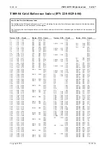
Page 71: ...ation IPN Section Page 220 01253 01 Parts List 14 2 2 Mechanical Miscellaneous Parts 14 2 5 Grid Reference Index 14 2 7 PCB Layout Bottom Side 14 2 11 PCB Layout Top Side 14 2 12 Processor Memory Regulators Circuit Diagram 14 2 13 Analogue I O Conversion Circuit Diagram 14 2 14 Serial Comms Digital I O Circuit Diagram 14 2 15 ...

Page 72: ...AP ELECT RADL 10UF 16V 4X7MM C170 020 09470 07 CAP 470M 16V 20 ELEC VERT 8 20 3 5MM L C171 020 09470 07 CAP 470M 16V 20 ELEC VERT 8 20 3 5MM L C201A 019 55100 01 CAP MONOLITHIC AI 10N 5 COG 50V C201B 022 54100 10 CAP MYLAR AI 1N 5 63V POTTED C201C 022 54100 10 CAP MYLAR AI 1N 5 63V POTTED C202A 019 55100 01 CAP MONOLITHIC AI 10N 5 COG 50V C202B 020 09220 06 CAP ELECT RADL 220M 16V 8X11 2MM C202C 0...

Page 73: ...iscellaneous Parts 14 3 5 Grid Reference Index 14 3 7 PCB Layout Bottom Side 14 3 9 PCB Layout Top Side 14 3 10 Circuit Diagram Sheet 1 14 3 11 Circuit Diagram Sheet 2 14 3 12 220 01254 04 Parts List 14 3 13 Mechanical Miscellaneous Parts 14 3 16 Grid Reference Index 14 3 17 PCB Layout Bottom Side 14 3 19 PCB Layout Top Side 14 3 20 Circuit Diagram Sheet 1 14 3 21 Circuit Diagram Sheet 2 14 3 22 ...

Page 74: ...0 08560 09 CAP ELECT RADL 56M 50V 6 3X15 5MM L S C61 020 07100 05 CAP ELECT RADL 1UF 50V 4X7MM C62 020 07100 05 CAP ELECT RADL 1UF 50V 4X7MM C63 019 55100 01 CAP MONOLITHIC AI 10N 5 COG 50V C64 019 55100 01 CAP MONOLITHIC AI 10N 5 COG 50V C65 022 56100 10 CAP MYLAR AI 100N 5 63V POTTED C66 022 56100 10 CAP MYLAR AI 100N 5 63V POTTED C67 020 09100 03 CAP ELECT RADL 100M 16V 8X11MM C68 020 08560 09 ...

Page 75: ... 52100 01 CAP CER AI 10P 5 NPO 50 63V C45 011 52100 01 CAP CER AI 10P 5 NPO 50 63V C46 020 08100 04 CAP ELECT RADL 10UF 16V 4X7MM C47 011 52100 01 CAP CER AI 10P 5 NPO 50 63V C48 011 52100 01 CAP CER AI 10P 5 NPO 50 63V C49 020 09100 03 CAP ELECT RADL 100M 16V 8X11MM C50 020 09100 03 CAP ELECT RADL 100M 16V 8X11MM C51 011 52100 01 CAP CER AI 10P 5 NPO 50 63V C52 022 54100 10 CAP MYLAR AI 1N 5 63V ...

Page 76: ...R 3 WAY 1 ROW PCB MTG LK6 2A 240 00020 59 HEADER 3 WAY 1 ROW PCB MTG LK6 2B 240 00020 59 HEADER 3 WAY 1 ROW PCB MTG LK7A 240 00020 59 HEADER 3 WAY 1 ROW PCB MTG LK7B 240 00020 59 HEADER 3 WAY 1 ROW PCB MTG LK7C 240 00020 59 HEADER 3 WAY 1 ROW PCB MTG PL1 240 00025 37 CONN MALE 34 WAY IDC PL2 240 02010 85 SKT 9 WAY PCB MOUNT STRAIGHT PL3 240 00025 37 CONN MALE 34 WAY IDC PL10 240 00020 51 PLUG 12 W...

Page 77: ...81 CONN 32 WAY DIN 41612 FEMALE SK3 240 02010 81 CONN 32 WAY DIN 41612 FEMALE SK4 240 02010 81 CONN 32 WAY DIN 41612 FEMALE SK5 240 02010 81 CONN 32 WAY DIN 41612 FEMALE SK6 240 02010 81 CONN 32 WAY DIN 41612 FEMALE SK7 240 02010 81 CONN 32 WAY DIN 41612 FEMALE SK8 240 02010 81 CONN 32 WAY DIN 41612 FEMALE SK9 240 02010 81 CONN 32 WAY DIN 41612 FEMALE SK10 240 04020 51 SKT 12 WAY 2 ROW 2X6 PCB MTG...

Page 78: ...Z For securing PCB to rack 345 00030 04 SCREW M2 6x8MM PAN PHILIPS NI PLT For securing SK1 SK9 to PCB 345 00030 20 SCREW M2 5x8MM BLACK CSK POZI MACHINE SCREW For securing spacer insulator between PCB and rack 345 00040 10 SCREW M3x6MM PAN POZI ST BZ For mounting REG1 REG2 and REG3 345 00050 07 SCREW M4x10MM PAN POZI ST BZ For securing front panel earth strap 352 00010 05 NUT M2 6 MACH HEX ST NI P...

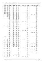
Page 79: ...N1 3 1 W6 1 E4 1 E4 1 E2 CN1 4 1 W5 1 E0 CN2 1 1 T4 1 G9 1 G8 1 G7 CN2 3 1 T6 1 G4 1 G4 1 G2 CN2 4 1 T5 1 G0 CN3 1 1 R4 1 I9 1 I8 1 I7 CN3 3 1 R6 1 I4 1 I4 1 I2 CN3 4 1 R5 1 I0 CN4 1 1 N4 1 K9 1 K8 1 K7 CN4 3 1 N6 1 K4 1 K4 1 K2 CN4 4 1 N5 1 K0 CN5 1 1 L4 1 M9 1 M8 1 M7 CN5 3 1 L6 1 M4 1 M4 1 M2 CN5 4 1 L5 1 M0 CN6 1 1 J4 1 O9 1 O8 1 O7 CN6 3 1 J6 1 O4 1 O4 1 O2 CN6 4 1 J5 1 O0 CN7 1 1 F4 1 Q9 1 Q...

Page 80: ...9 2 S6 R69 1 D9 2 T5 R70 1 D9 2 U5 R71 1 D9 2 U6 R72 1 D10 2 U5 R73 1 D10 2 U5 R74 1 D9 2 V5 R75 1 D10 2 V4 R76 1 D9 2 V6 R77 1 C10 2 V5 R78 1 D10 2 U4 R79 1 F11 2 I6 R80 1 E11 2 J5 R81 1 E11 2 J5 R82 1 E11 2 J6 R83 1 E11 2 J5 R84 1 E10 2 K6 R85 1 E11 2 K5 R86 1 E11 2 K5 R87 1 E11 2 K6 R88 1 D11 2 L5 R89 1 D11 2 M5 R90 1 D11 2 M6 R91 1 D12 2 M5 R92 1 D12 2 M5 R93 1 D11 2 N5 R94 1 D12 2 N4 R95 1 D1...

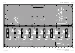
Page 81: ...M805 00 T805 04 PCB Information 14 3 19 Copyright TEL 30 09 96 T805 04 PCB Layout Bottom Side 220 01254 04 ...

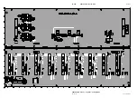
Page 82: ...14 3 20 T805 04 PCB Information M805 00 30 09 96 Copyright TEL T805 04 PCB Layout Top Side 220 01254 04 ...

Page 83: ... 3 LK3 8B 3 WAY PLUG 1 2 3 LK3 9A 3 WAY PLUG 1 2 3 LK3 9B 3 WAY PLUG 1 2 3 LK5 1A 3 WAY PLUG 1 2 3 LK5 1B 3 WAY PLUG 1 2 3 LK5 2A 3 WAY PLUG 1 2 3 LK5 2B 3 WAY PLUG 1 2 3 LK6 1A 3 WAY PLUG 1 2 3 LK6 1B 3 WAY PLUG 1 2 3 LK6 2A 3 WAY PLUG 1 2 3 LK6 2B 3 WAY PLUG 1 2 3 R1 680 R11 680 R12 680 R13 680 R14 680 R15 680 R16 680 R17 680 R18 680 R19 680 R2 680 R21 1K0 R22 1K0 R3 680 R4 680 R5 680 R6 680 R7 ...

Page 84: ...T SK4 2X16 WAY TOP ENTRY SKT SK5 2X16 WAY TOP ENTRY SKT SK6 2X16 WAY TOP ENTRY SKT SK7 2X16 WAY TOP ENTRY SKT SK8 2X16 WAY TOP ENTRY SKT SK9 2X16 WAY TOP ENTRY SKT SW1 SPST 1 2 3 PL1 DGND 27 PL1 DGND 33 PL1 DGND 34 PL1 DGND 28 PL1 GND 25 PL1 GND 26 PL1 GND 11 PL1 GND 18 PL1 GND 24 PL1 GND 23 PL1 GND 17 PL1 GND 19 PL1 GND 20 PL1 GND 10 PL1 GND 12 PL1 GND 15 PL1 GND 3 PL1 GND 4 PL1 GND 5 PL1 GND 6 P...

Page 85: ...DER 3 WAY 1 ROW PCB MTG LINK3 240 00020 59 HEADER 3 WAY 1 ROW PCB MTG R1 030 54100 20 RES FILM AI 1K 5 0 4W 4X1 6MM R2 030 53680 20 RES FILM AI 680E 5 0 4W 4X1 6MM R3 030 53680 20 RES FILM AI 680E 5 0 4W 4X1 6MM R4 030 53680 20 RES FILM AI 680E 5 0 4W 4X1 6MM R5 030 53680 20 RES FILM AI 680E 5 0 4W 4X1 6MM R6 030 53680 20 RES FILM AI 680E 5 0 4W 4X1 6MM R7 030 53100 20 RES FILM AI 100E 5 0 4W 4X1 ...

Page 86: ... POZI ST BZ 352 00010 08 NUT M3 COLD FORM HEX ST BZ 353 00010 11 WASHER M3 FLAT 9 5MM 0 9MM ST BZ 353 00010 13 WASHER M3 SHAKEPROOF INT BZ Audio Power PCB to U Rack 356 00020 06 RECEPTL 6 3MM QUICK CONNECT FLARED INSULAT 360 00010 11 GROMMET FLAT CORD CLAMPING TYPE B 362 00010 13 BUSH INSULATING 1 1MM TOP HAT 365 00100 20 LABEL WHITE S A 28X11MM QUIKSTIK RW718 4 365 01376 00 LABEL A4A724 SOFTWARE ...

Page 87: ... Front Panel PCB Information 14 5 1 14 5 T805 Front Panel PCB This section contains the following information IPN Section Page 220 01354 00 Parts List 14 5 2 Circuit Diagram 14 5 4 PCB Layout Top Side 14 5 5 PCB Layout Bottom Side 14 5 6 ...

Page 88: ...G LED8 008 00011 52 S LED 5MM RED DIFFUSED HI INTENSITY NO MTG LED9 008 00011 52 S LED 5MM RED DIFFUSED HI INTENSITY NO MTG PL1 240 00020 51 PLUG 12 WAY 2X6 FLAT CABLE TERMN R1 030 55220 20 RES FILM AI 22K 5 0 4W 4X1 6MM R2 030 54100 20 RES FILM AI 1K 5 0 4W 4X1 6MM R3 030 55220 20 RES FILM AI 22K 5 0 4W 4X1 6MM R4 030 54100 20 RES FILM AI 1K 5 0 4W 4X1 6MM R5 030 55220 20 RES FILM AI 22K 5 0 4W 4...

Page 89: ...Copyright TEL 30 09 96 M805 00 T805 Front Panel PCB Information 14 5 3 ...

Page 90: ... IC2 74F04 5 6 IC2 74F04 9 8 IC2 74F04 11 10 IC2 74F04 1 2 IC2 74F04 3 4 IC2 74F04 13 12 LED1 RED LED2 RED LED3 RED LED4 RED LED5 RED LED6 RED LED7 RED LED8 RED LED9 RED R1 22K R10 1K0 R11 22K R12 1K0 R13 22K R14 1K0 R15 22K R16 1K0 R17 22K R18 1K0 R2 1K0 R3 22K R4 1K0 R5 22K R6 1K0 R7 22K R8 1K0 R9 22K SK1 2X6 WAY TOP ENTRY SKT SW1 SPDT 1 2 3 SW2 SPDT 1 2 3 SW3 SPDT 1 2 3 SW4 SPDT 1 2 3 SW5 SPDT ...

Page 91: ...M805 00 T805 Front Panel PCB Information 14 5 5 Copyright TEL 30 09 96 T805 Front Panel PCB Layout Top Side 220 01354 00 ...

Page 92: ...14 5 6 T805 Front Panel PCB Information M805 00 30 09 96 Copyright TEL T805 Front Panel PCB Layout Bottom Side 220 01354 00 ...

Page 93: ...ine polarity reversals and amplitude variations of the land line Amplitude Response The variation in amplitude of a signal as its fre quency is changed ARM Audio Recovery Module T805 01 A complement to the AIM ASP Card Audio Signal Processing card The hardware description for the cards used in the Quasi Synchro nous system An ASP card can be a TSGM LEM AIM or ARM depending on the software used Bre...

Page 94: ...transmit audio over a digital link Inversion Mode The most common operating mode of an AIM when in use The audio passed into it is mixed around a carrier and thus baseband shifted This mode is used so that signals in the 67 300Hz frequency range may be passed down a land line which has a very poor frequency response below 300Hz Land Line A means of linking communications between two physically sep...

Page 95: ...on the same fre quency whose transmission areas may overlap Another name for Simulcast system Recovery Mode The most common operating mode of an ARM when in use Used to reverse the process carried out in an AIM RIC A single unit in an ICCS system which performs the A D conversion and passes the data onto the digital transmission link It is also capable of converting a digital signal back to audio ...

Page 96: ...hat occur as the speech audio is passed to the transmitters in the Quasi Synchronous system TSGM Test Signal Generator Module T805 03 The unit that provides the training signals which the LEMs use to equalise their path in the Quasi Synchronous system Voting Testing the RF signal strength of received signals to determine which is strongest ...

Reviews: