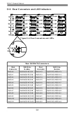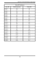
D-5
Appendix D: SAS-846A Backplane Specifications
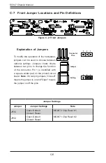
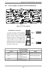
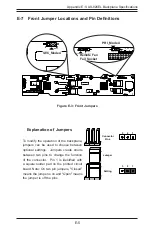
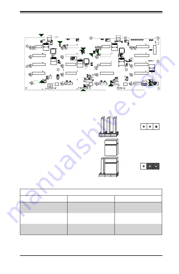
D-7 Front Jumper Locations and Pin Definitions
Explanation of Jumpers
To modify the operation of the backplane,
jumpers can be used to choose between
optional settings. Jumpers create shorts
between two pins to change the function
of the connector. Pin 1 is identified with
a square solder pad on the printed circuit
board. Note: On two pin jumpers, "Closed"
means the jumper is on and "Open" means
the jumper is off the pins.
Connector
Pins
Jumper
Setting
3 2 1
3 2 1
Figure D-2: Front Jumpers
BZ1
+
+
DESIGNED IN USA
SAS846A
REV: 1.00
C319
C194
C282
C35
C135
C136
C149
C243
C258
C261
C272
C88
C271
C89
C106
C206
C241
C212
C213
C337
C359
R325
R105
R324
R111
R414
R415
R148
R112
R147
R344
R104
R113
R305
R367
R167
R184
R127
R183
R128
R185
R168
R270
R494
R575
R591
R619
R623
R624
R629
R220
R219
R218
R217
R425
R424
R423
R405
R404
R403
Y3
Y2
Y1
JSM1
JSM2
JSM3
JSM4
JSM5
JSM6
F14
F19
F20
F5
F6
4
1
JP60
4
1
JP58
4
1
4
1
JP54
MH15
MH14
MH13
MH12
MH11
U63
JP108
JP47
JP26
U2
JP115
JP78
JP69
U91
U24
JP116
JP117
JP52
JP96
JP95
JP37
JP10
JP13
JP46
JP48
+5V
+12V
GND
GND
JP109
+5V
+12V
GND
GND
JP110
JP105
JP106
D64
D113
D116
JP64
1
3
JP63
1
3
JP62
1
3
JP61
JP50
1
3
JP35
1
JP129
1
3
JP107
1
3
JP97
JP98
JP99
JP45
JP25
JP100
JP18
F4
D54
A
C
D53
A
C
D36
A
C
D3
A
C
D51
A
C
D49
A
C
D47
A
C
D45
A
C
D89
A
C
C85
C84
C5
C45
C44
C3
C204
+
C203
C202
C201
C200
C199
C198
C197
C119
C285
C330
+
C329
+
C328
+
C327
+
C326
+
C325
+
C324
+
C323
+
C283
C229
C20
C193
C19
C173
C318
1
16
49
64
U73
U40
U19
I2C#2
CH#20~23
CH#12~15
CH#8~11
CH#4~7
2-3:I2C
1-2:SGPIO
JP84:MODE
+
2-3: NO RESET
1-2: RESET
2-3: NO RESET
1-2: RESET
2-3: NO RESET
1-2: RESET
22
23
20
21
18
19
16
17
14 15
12 13
10 11
8 9
6
7
4
5
3
2
1
0
+
+
+
+
+
+
+
+
+
+
+
+
+
+
+
JP129:9072#3 RESET
JP35:9072#1 RESET
JP50:9072#2 RESET
BUZZER RESET
2-3:NO FAN
1-2:WITH FAN
JP61:FAN#1 SELECT
JP64:FAN#4 SELECT
JP63:FAN#3 SELECT
JP62:FAN#2 SELECT
2-3:NO FAN
1-2:WITH FAN
JP97:FAN#1 SELECT
JP98:FAN#2 SELECT
JP99:FAN#3 SELECT
JP100:FAN#4 SELECT
C
C
C
OPEN:45
1-2:50
2-3:55
JP107:OH#3 TEMP.
ACT_IN#16-23
ACT_IN#8-15
AC
T_IN#0-7
UPGR
ADE#3
UPGR
ADE#1
I2C#5
I2C#6
I2C#3
CH#0~3
I2C#1
FAN#4
FAN#3
FAN#2
FAN#1
#23
#22
#21
#20
#19
#18
#17
#16
#15
#14
#13
#12
#11
#10
#9
#5
#4
#3
#2
#1
#0
C
C
C
1-2:50
OPEN:45
JP25:OH#1 TEMP.
2-3:55
JP45:OH#2 TEMP.
C
2-3:55
1-2:50
C
C
OPEN:45
JP129
JP50
JP35
JP97
JP100
JP18
JP99
JP98
JP64
JP84
JP63
JP62
JP61
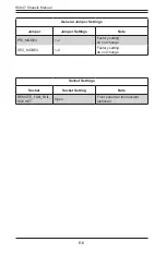
Jumper Settings
Jumper
Jumper Setting
Notes
JP35
1-2: Reset
2-3: Normal (Default)
MG9072 Chip Reset #1
JP50
1-2: Reset
2-3: Normal (Default)
MG9072 Chip Reset #2
JP129
1-2: Reset
2-3: Normal (Default)
MG9072 Chip Reset #3
Summary of Contents for SC847 Series
Page 12: ...SC847 Chassis Manual 1 4 Notes...
Page 32: ...2 20 SC847 Chassis Manual Notes...
Page 53: ...5 15 Chapter 5 Chassis Setup and Maintenance Figure 5 14 Placing the System Fan...
Page 76: ...SC847 Chassis Manual B 2 Notes...
Page 86: ...C 10 SC847 Chassis Manual Notes...
Page 96: ...D 10 SC847 Chassis Manual Notes...
Page 118: ...E 22 SC847 Chassis Manual Notes...
Page 187: ...H 23 Appendix H SAS2 846EL Backplane Specifications Notes...

