1-18
IC
VGN-
S36C/S36GP/S36LP/S36SP/S36TP/S38CP/
S52B/
S62PS/S62PSY/S62S/
S350F/S350FP/
S360/S360P/
S370F
(J/AM
/AO
)
Confidential
IN
SYNC
Power
On
Reset
Shoot-through
Protection
VCC
LG
GND
Logic
Q
1
Q
2
BOOT
HG
SW
+4V ~ +7V
+
-
VIN (up to 33V)
VOUT
Items in bold
are external
to the IC.
6
µ
A
VCC
6
µ
A
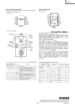
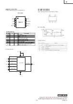
Pin Description
Pin #
Pin Name
Pin Function
1
SW
Top driver return. Should be connected to the common node of top and bottom FETs.
2
HG
Top gate drive output. Should be connected to the top FET gate.
3
BOOT
Bootstrap. Accepts a bootstrap voltage for powering the high-side driver.
4
IN
Accepts a logic control signal.
5 SYNC
Bottom
gate
enable.
6
VCC
Connect to +5V supply.
7
LG
Bottom gate drive output. Should be connected to bottom FET gate.
8 GND
Ground.
Block Diagram
Electrical Characteristics
LM2724
VCC = BOOT = SYNC = 5V, SW = GND = 0V, unless otherwise specified. Typicals and limits appearing in plain type
apply for T
A
= T
J
= +25
°
C. Limits appearing in
boldface
type apply over the entire operating temperature range.
Symbol Parameter
Conditions
Min
Typ
Max
Units
POWER SUPPLY
I
q_op
Operating Quiescent Cur-
rent
IN = 0V.
142
195
µ
A
TOP DRIVER
Peak Pull-up Current
3.0 A
Pull-up
Rds_on
I
BOOT
= I
HG
= 0.7A
1.2
Ω
Peak Pull-down Current
-3.2 A
Pull-down
Rds_on I
SW
= I
HG
= 0.7A
0.5
Ω
t
4
Rise Time
Timing Diagram, C
LOAD
= 3.3nF
17
ns
t
6
Fall Time
Timing Diagram, C
LOAD
= 3.3nF
12
ns
t
3
Pull-up Dead Time
Timing Diagram
19
ns
t
5
Pull-down Delay
Timing Diagram, IN
↓
.
27
ns
BOTTOM DRIVER
Peak Pull-up Current
3.2 A
Pull-up
Rds_on
I
VCC
= I
LG
= 0.7A
1.1
Ω
Peak Pull-down Current
3.2 A
Pull-down
Rds_on I
GND
= I
LG
= 0.7A
0.6
Ω
Electrical Characteristics (continued)
LM2724
VCC = BOOT = 5V, SW = GND = 0V, unless otherwise specified. Typicals and limits appearing in plain type apply for T
A
= T
J
= +25
°
C. Limits appearing in
boldface
type apply over the entire operating temperature range.
Symbol Parameter
Conditions
Min
Typ
Max
Units
t
8
Rise Time
Timing Diagram, C
LOAD
= 3.3nF
17
ns
t
2
Fall Time
Timing Diagram, C
LOAD
= 3.3nF
14
ns
t
7
Pull-up Dead Time
Timing Diagram
22
ns
t
1
Pull-down Delay
Timing Diagram
13
ns
LOGIC
V
uvlo_up
VCC Under-Voltage-Lock-
Out Upper Threshold
VCC rises from 0V toward 5V
4
V
V
uvlo_dn
VCC Under-Voltage-Lock-
Out Lower Threshold
VCC falls from 5V toward 0V
2.5
V
V
uvlo_hys
VCC Under-Voltage-Lock-
Out Hysteresis
VCC falls from 5V toward 0V
0.8
V
V
IH_SYNC
SYNC Pin High Input
55%
V
IL_SYNC
SYNC Pin Low Input
25%
VCC
SYNC = 5V, sink current
2
I
leak_SYNC
SYNC Pin Leakage Cur-
rent
SYNC = 0V, source current
10
µ
A
IN = 5V, sink current
10
I
leak_IN
IN Pin Leakage Current
IN = 0V, source current
2
µ
A
t
on_min
Minimum Positive Output
Pulse Width (Note 4)
50
ns
t
off_min
Minimum Negative Output
Pulse Width (Note 5)
50
ns
t
IN_min
Minimum Pulse Width at
the IN Pin
5
ns
V
IH_IN
IN High Level Input Volt-
age
When IN pin goes high from 0V
55%
V
IL_IN
IN Low Level Input Volt-
age
When IN pin goes low from 5V
25%
VCC
Note 1: Absolute Maximum Ratings
are limits beyond which damage to the device may occur. Operating ratings are
conditions under which the device operates correctly.
Operating Ratings
do not imply guaranteed performance limits.
Note 2:
Maximum allowable power dissipation is a function of the maximum junction temperature, T
JMAX
, the junction-to-
ambient thermal resistance,
θ
JA
, and the ambient temperature, T
A
. The maximum allowable power dissipation at any
ambient temperature is calculated using:
P
MAX
=(T
JMAX
-T
A
) /
θ
JA
. The junction-to-ambient thermal resistance,
θ
JA
, for the
LM2724 SO-8 package is 172
°
C/W. For a T
JMAX
of 150
°
C and T
A
of 25
°
C, the maximum allowable power dissipation is
0.7W. The
θ
JA
for the LM2724 LLP-8 package is 39
°
C/W. For a T
JMAX
of 150
°
C and T
A
of 25
°
C, the maximum allowable
power dissipation is 3.2W.
Note 3:
ESD machine model susceptibility is 200V.
Note 4:
Whenever the LM2724 sees a rising edge at the IN pin after IN has been low for at least t
off_min
, the high-side
driver will be turned on for at least t
on_min
. Otherwise the edge will be ignored.
Note 5:
Whenever the LM2724 sees a falling edge at the IN pin after IN has been high for at least t
on_min
, the low-side
driver will be turned on for at least t
off_min
. Otherwise the edge will be ignored.
Note 6:
At the IN pin, if a falling edge is followed by a rising edge within 5ns, the HG may ignore the rising edge and re-
main low until the IN pin toggles again. If a rising edge is followed by a falling edge within 5ns, the pulse may be com-
pletely ignored.


