


1-36
IC
VGN-
S36C/S36GP/S36LP/S36SP/S36TP/S38CP/
S52B/
S62PS/S62PSY/S62S/
S350F/S350FP/
S360/S360P/
S370F
(J/AM
/AO
)
Confidential
Signal Name
Type
Description
G_DEVSEL#
I/O
s/t/s
AGP
G_ DEVSEL#:
Device Select.
During PIPE# and SBA Operation:
This signal is not used during PIPE# or SBA
operation.
During FRAME# Operation:
G_DEVSEL#, when asserted, indicates that a
FRAME#-based AGP target device has decoded its address as the target of the
current access. The MCH asserts G_DEVSEL# based on the SDRAM address
range being accessed by a PCI initiator. As an input, G_DEVSEL# indicates
whether the AGP master has recognized a PCI cycle to it.
G_REQ#
I
AGP
G_REQ#:
Request.
During SBA Operation:
This signal is not used during SBA operation.
During PIPE# and FRAME# Operation:
G_REQ#, when asserted, indicates that
the AGP master is requesting use of the AGP interface to run a FRAME#- or
PIPE#-based operation.
G_GNT#
O
AGP
G_GNT#:
Grant.
During SBA, PIPE# and FRAME# Operation:
G_GNT#, along with the information
on the ST[2:0] signals (status bus), indicates how the AGP interface will be used
next. Refer to the
AGP Interface Specification, Revision 2.0
for further explanation
of the ST[2:0] values and their meanings.
G_AD[31:0]
I/O
AGP
G_AD[31:0]:
Address/Data Bus.
During PIPE# and FRAME# Operation:
The G_AD[31:0] signals are used to
transfer both address and data information on the AGP interface.
During SBA Operation:
The G_AD[31:0] signals are used to transfer data on the
AGP interface.
G_CBE[3:0]#
I/O
AGP
Command/Byte Enable.
During FRAME# Operation:
During the address phase of a transaction, the
G_CBE[3:0]# signals define the bus command. During the data phase, the
G_CBE[3:0]# signals are used as byte enables. The byte enables determine which
byte lanes carry meaningful data. The commands issued on the G_CBE# signals
during FRAME#-based AGP transactions are the same G_CBE# command
described in the PCI 2.2 specification.
During PIPE# Operation:
When an address is enqueued using PIPE#, the C/BE#
signals carry command information. Refer to the
AGP 2.0 Interface Specification,
Revision 2.0
for the definition of these commands. The command encoding used
during PIPE#-based AGP is
different
than the command encoding used during
FRAME#-based AGP cycles (or standard PCI cycles on a PCI bus).
During SBA Operation:
These signals are not used during SBA operation.
G_PAR
I/O
AGP
Parity.
During FRAME# Operation:
G_PAR is driven by the MCH when it acts as a
FRAME#-based AGP initiator during address and data phases for a write cycle, and
during the address phase for a read cycle. G_PAR is driven by the MCH when it
acts as a FRAME#-based AGP target during each data phase of a FRAME#-based
AGP memory read cycle. Even parity is generated across G_AD[31:0] and
G_CBE[3:0]#.
During SBA and PIPE# Operation:
This signal is not used during SBA and PIPE#
operation.
PCIRST# from the ICH4-M is assumed to be connected to RSTIN# and is used to reset AGP interface
logic within the MCH. The AGP agent will also typically use PCIRST# provided by the ICH4-M as an
input to reset its internal logic.
2.5.
Clocks, Reset, and Miscellaneous
Table 12. Clocks, Reset, and Miscellaneous Signal Descriptions
Signal Name
Type
Description
BCLK
BCLK#
I
CMOS
Differential Host Clock In:
These pins receive a differential host clock from the
external clock synthesizer. This clock is used by all of the MCH logic that is in the
Host clock domain.
66IN
I
CMOS
66 MHz Clock In:
This pin receives a 66-MHz clock from the clock synthesizer.
This clock is used by AGP/PCI and hub interface clock domains.
NOTE:
That this clock input is 3.3-V tolerant.
SCK[5:0]
O
CMOS
SDRAM Differential Clock (DDR):
These signals deliver a source synchronous
clock to the SO-DIMMs. There are three per SO-DIMM.
SCK#[5:0]
O
CMOS
SDRAM Inverted Differential Clock (DDR):
These signals are the complement to
the SCK[5:0] signals. There are three per SO-DIMM.
RSTIN#
I
CMOS
Reset In:
When asserted this signal will asynchronously reset the MCH logic. This
signal is connected to the PCIRST# output of the ICH4-M. All AGP/PCI output and
bi-directional signals will also tri-state compliant to PCI Rev 2.0 and 2.1
specifications.
NOTE:
That this input needs to be 3.3-V tolerant.
TESTIN#
I
CMOS
Test Input:
This pin is used for manufacturing and board level test purposes.
NOTE:
This signal has an internal pullup resistor.
DPSLP#
I
CMOS
Deep Sleep Input:
This signal comes from the ICH4-M device, providing an
indication of C3 and Deeper Sleep (C4) state entry to the CPU.
NOTE:
that this input is low-voltage CMOS, operating on the PSB Vccp power
plane.
ETS#
I
CMOS
External Thermal Sensor Input:
This signal is an active low input to the MCH,
which is used to monitor status of external thermal sensor activity, is enabled. The
MCH can be optionally programmed to send a SERR, SCI, or SMI message to
ICH4-M upon the triggering of this signal.
2.6.
Voltage References, PLL Power
Table 13. Voltage References, PLL Power Descriptions
Signal Name
Type
Description
HLRCOMP
I/O
CMOS
Compensation for hub interface:
This signal is used to calibrate the hub
interface I/O buffers.
GRCOMP
I/O
CMOS
Compensation for AGP:
This signal is used to calibrate AGP buffers.
HRCOMP[1:0]
I/O
CMOS
Compensation for Host:
This signal is used to calibrate the Host AGTL+ I/O
buffers.
SMRCOMP
I/O
CMOS
System Memory RCOMP
HVREF[4:0]
Host Reference Voltage.
Reference voltage input for the Data, Address, and
Common clock signals of the Host AGTL+ interface
SMVREF[1:0]
DDR Reference Voltage:
Reference voltage input for DQ, DQS, and RCVENIN#.
HI_REF
Hub Interface Reference:
Reference voltage input for the hub interface.
AGPREF
AGP Reference:
Reference voltage input for the AGP interface.
HSWNG[1:0]
Host Reference Voltage:
Reference voltage input for the compensation logic.
VCC1_2
The 1.2 V Power input pins
VCC1_8
The 1.8 V Power input pins
VCCSM
The DRAM Power input pins.
2.5 V for DDR.
VCC1_5
The power supply input for the AGP I/O supply (1.5 V)
VCCGA,
VCCHA
PLL power input pins. (1.8 V)
VCCP
The AGTL+ bus termination voltage inputs (1.05 V)
VSS
GROUND
The following table shows the value of the RCOMP resistor and the termination point for each
interface’s RCOMP signal.
Note:
These values are based on the board impedance assumption of 55 Ohm ± 15%.
Table 14. RCOMP Resistor Value Recommendations
Interface
RCOMP R
RCOMP Term
Host PSB
27.4 Ohm ± 1%
VSS
AGP
36.5 Ohm ± 1%
VSS
Hub Interface
39.4 Ohm ± 1%
VCC1_8
SM DDR
30.1 Ohm ± 1%
V1.25
(1.25 V Vtt for DDR)
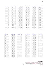
9.2.
Ballout Table
Signal Name
Ball#
ADS# U7
AD_STB0 R24
AD_STB1 AC27
AD_STB0# R23
AD_STB1# AC28
AGPREF AA21
BNR# V3
BPRI# Y7
BR0# V7
CPURST# AE17
DBSY# V5
DEFER# Y4
DBI0# AD5
DBI1# AG5
DBI2# AH9
DBI3# AD15
DPSLP# V8
DPWR# Y8
DRDY# W2
G_AD0 R27
G_AD1 R28
G_AD10 T23
G_AD11 U23
G_AD12 T24
G_AD13 U24
G_AD14 U25
G_AD15 V24
G_AD16 Y27
G_AD17 Y26
G_AD18 AA28
G_AD19 AB25
G_AD2 T25
G_AD20 AB27
Signal Name
Ball#
G_AD21 AA27
G_AD22 AB26
G_AD23 Y23
G_AD24 AB23
G_AD25 AA24
G_AD26 AA25
G_AD27 AB24
G_AD28 AC25
G_AD29 AC24
G_AD3 R25
G_AD30 AC22
G_AD31 AD24
G_AD4 T26
G_AD5 T27
G_AD6 U27
G_AD7 U28
G_AD8 V26
G_AD9 V27
G_CBE0# V25
G_CBE1# V23
G_CBE2# Y25
G_CBE3# AA23
66IN P22
G_DEVSEL# W28
G_FRAME# Y24
G_GNT# AH25
G_IRDY# W27
G_PAR W25
GRCOMP AD25
G_REQ# AG24
G_STOP# W23
G_TRDY# W24
HA10# P4
Signal Name
Ball#
HA11# P3
HA12# P5
HA13# R6
HA14# N2
HA15# N5
HA16# N3
HA17# J3
HA18# M3
HA19# M4
HA20# M5
HA21# L5
HA22# K3
HA23# J2
HA24# N6
HA25# L6
HA26# L2
HA27# K5
HA28# L3
HA29# L7
HA3# U6
HA30# K4
HA31# J5
HA4# T5
HA5# R2
HA6# U3
HA7# R3
HA8# P7
HA9# T3
HADSTB0# R5
HADSTB1# N7
BCLK# K8
BCLK J8
HD0# AA2