


1-42
IC
VGN-
S36C/S36GP/S36LP/S36SP/S36TP/S38CP/
S52B/
S62PS/S62PSY/S62S/
S350F/S350FP/
S360/S360P/
S370F
(J/AM
/AO
)
Confidential
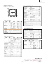
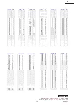
Table 2−3. 16-Bit PC Card Signal Names Sorted Alphabetically (Continued)
SIGNAL NAME
TERMINAL
NUMBER
SIGNAL NAME
TERMINAL
NUMBER
SIGNAL NAME
TERMINAL
NUMBER
SIGNAL
NAME
TERMINAL
NUMBER
B_CE2
L15
FILTER0
U17
MS_DATA2
G03
TEST0
R19
B_D0
A17
FILTER1
U18
MS_DATA3
H07
TPA0N
W14
B_D1
E14
GND
H08
MS_SDIO(DATA0)
G01
TPA0P
V14
B_D2
C15
GND
H09
NC
M12
TPA1N
W18
B_D3
P17
GND
H11
NC
N13
TPA1P
V18
B_D4
P19
GND
J09
NC
P14
TPBIAS0
U14
B_D5
M15
GND
J10
NC
P15
TPBIAS1
V19
B_D6
N18
GND
J11
NC
R14
TPB0N
W13
B_D7
L13
GND
J12
NC
U16
TPB0P
V13
B_D8
B16
GND
K09
PAR
N09
TPB1N
W16
B_D9
A16
GND
K10
PCLK
R01
TPB1P
V16
B_D10
E13
GND
K11
PC0(TEST1)
N12
TRDY
V06
B_D11
P18
GND
L08
PC1(TEST2)
U12
V
CC
G07
B_D12
M14
GND
L09
PC2(TEST3)
V12
V
CC
G08
B_D13
N17
GND
L10
PERR
U07
V
CC
G11
B_D14
N19
GND
L11
PHY_TEST_MA
R17
V
CC
G12
B_D15
M19
GND
L12
PRST
P03
V
CC
G13
B_INPACK
E17
GND
M08
REQ
T01
V
CC
H10
B_IORD
L17
GND
M09
RI_OUT/PME
R03
V
CC
H12
B_IOWR
K13
GND
M10
RSVD
H05
V
CC
J08
B_OE
L19
GND
U09
RSVD
J05
V
CC
K08
B_READY(IREQ)
B19
GNT
R02
RSVD
J06
V
CC
K12
B_REG
D18
GRST
N05
RSVD
K01
V
CC
M07
B_RESET
E19
IDSEL
V03
RSVD
K02
V
CC
M11
B_WAIT
B18
IRDY
U06
RSVD
K03
V
CC
M13
B_WE
H19
LATCH
M02
R0
W15
V
CC
N08
B_WP(IOIS16)
B17
MC_CD_0
E02
R1
V15
V
CCA
A04
B_VS1
C18
MC_CD_1
E01
SCL
K07
V
CCA
A10
B_VS2
F18
MC_PWR_CTRL_0
F01
SDA
L03
V
CCB
D19
CLK_48
L02
MC_PWR_CTRL_1
F03
SD_CLK
H01
V
CCB
K19
CLOCK
L05
MFUNC0
M03
SD_CMD
H02
V
CCP
V01
CNA
R18
MFUNC1
L06
SD_DAT0
H03
V
CCP
W08
CPS
P12
MFUNC2
N01
SD_DAT1
J07
VDPLL
U19
C/BE0
U10
MFUNC3
N02
SD_DAT2
J01
VR_EN
L01
C/BE1
P09
MFUNC4
N03
SD_DAT3
J02
VR_PORT
J19
C/BE2
R07
MFUNC5
M05
SD_WP
J03
VR_PORT
K05
C/BE3
W02
MFUNC6
P01
SERR
V07
VSPLL
T17
DATA
M01
MS_BS
F02
SPKROUT
L07
XI
T18
DEVSEL
R08
MS_CLK
G05
STOP
W06
XO
T19
FRAME
W05
MS_DATA1
G02
SUSPEND
P02
2.2
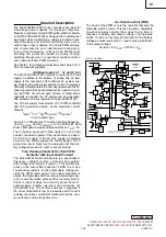
Detailed Terminal Descriptions
Please see Table 2−4 through Table 2−12 for more detailed terminal descriptions. The following list defines the
column headings and the abbreviations used in the detailed terminal description tables.
•
I/O Type:
−
I = Digital input
−
O = Digital output
−
I/O = Digital input/output
−
AI = Analog input
−
PWR = Power
−
GND = Ground
•
Input/Output Description:
−
AF = Analog feedthrough
−
TTLI1 = 5-V tolerant TTL input buffer
−
TTLI2 = 5-V tolerant TTL input buffer with hysteresis
−
TTLO1 = 5-V tolerant low-noise 4-mA TTL output buffer
−
PCII1 = 5-V tolerant PCI input buffer
−
PCII2 = 5-V tolerant PCI input buffer
−
PCII3 = 5-V tolerant PCI input buffer
−
PCII4 = 5-V tolerant PCI input buffer
−
PCII5 = 5-V tolerant PCI input buffer
−
PCIO2 = 5-V tolerant PCI output buffer
−
PCIO4 = 5-V tolerant PCI output buffer
−
PCIO5 = 5-V tolerant PCI output buffer
−
LVCI1 = LVCMOS input buffer
−
LVCO1 = Low-noise 4-mA LVCMOS open drain output buffer
−
LVCO2 = Low-noise 4-mA LVCMOS open drain output buffer
−
LVCO3 = Low-noise 8-mA LVCMOS open drain output buffer
•
PU/PD signifies whether the terminal has an internal pullup or pulldown resistor. These pullups are disabled
and enabled by design when appropriate to preserve power.
−
PD1 = 20-
µ
A failsafe pulldown
−
PD2 = 100-
µ
A failsafe pulldown
−
PU1 = 200-
µ
A pullup
−
PU2 = 100-
µ
A pullup
−
PU3 = 100-
µ
A pullup
−
PU4 = 100-
µ
A pullup
−
SW = Switchable 50-
µ
A pullup/200-
µ
A pulldown implemented depending on situation
•
Power Rail signifies which rail the terminal is clamped to for protection.
•
External Components signifies any external components needed for normal operation.
•
Pin Strapping (If Unused) signifies how the terminal must be implemented if its function is not needed.
The terminals are grouped in tables by functionality, such as PCI system function, power-supply function, etc. The
terminal numbers are also listed for convenient reference.
Table 2−4. Power Supply Terminals
Output description, internal pullup/pulldown resistors, and the power rail designation are not applicable for the power
supply terminals.
TERMINAL
I/O
EXTERNAL
PIN STRAPPING
NAME
NO.
DESCRIPTION
I/O
TYPE
INPUT
EXTERNAL
COMPONENTS
PIN STRAPPING
(IF UNUSED)
AGN2
AGN3
AGN4
U13
R13
W17
Analog circuit ground terminals
GND
−
−
NA
AVD2
AVD3
AVD4
R12
U15
V17
Analog circuit power terminals. A parallel combination of high frequency
decoupling capacitors near each terminal is suggested, such as 0.1
µ
F
and 0.001
µ
F. Lower frequency 10-
µ
F filtering capacitors are also recom-
mended. These supply terminals are separated from VDPLL and VSPLL
internal to the device to provide noise isolation. They must be tied to a
low-impedance point on the circuit board.
GND
−
−
NA
GND
H08, H09,
H11, J09,
J10, J11,
J12, K9,
K10, K11,
L08, L09,
L10, L11,
L12, M08,
M09, M10,
U09
Digital ground terminal
GND
−
−
NA
VCC
G07, G08,
G11, G12,
G13, H10,
H12, J08,
K08, K12,
M07, M11,
M13, N08
Power supply terminal for I/O and internal voltage regulator
PWR
−
−
NA
VCCA
A04, A10
Clamp voltage for PC Card A interface. Matches card A signaling envi-
ronment, 5 V or 3.3
PWR
−
−
Float
VCCB
D19, K19
Clamp voltage for PC Card B interface. Matches card B signaling envi-
ronment, 5 V or 3.3 V
PWR
−
−
Float
VCCP
W08, V01
Clamp voltage for PCI and miscellaneous I/O, 5 V or 3.3 V
PWR
−
−
NA
VDPLL
U19
PLL circuit power terminal. A parallel combination of high frequency
decoupling capacitors near the terminal is suggested, such as 0.1
µ
F
and 0.001
µ
F. Lower frequency 10-
µ
F filtering capacitors are also recom-
mended. This supply terminal is separated from AVDx internal to the
device to provide noise isolation. It must be tied to a low-impedance
point on the circuit board.
PWR
−
−
NA
VR_EN
L01
Internal voltage regulator enable. Active low.
AI
AF
Pull directly to
GND
NA
VR_PORT
J19, K05
1.8-V output from voltage regulator
PWR
−
0.1-
µ
F capacitor
to GND
NA
VSPLL
T17
This terminal must be tied to the low-impedance circuit board ground
plane.
GND
−
−
NA
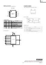
Table 2−5. PC Card Power Switch Terminals
Internal pullup/pulldown resistors, power rail designation, and pin strapping are not applicable for the power switch
terminals.
TERMINAL
I/O
NAME
NO.
DESCRIPTION
I/O
TYPE
INPUT
OUTPUT
EXTERNAL COMPONENTS
CLOCK
L05
Power switch clock. Information on the DATA line is sampled at the
rising edge of CLOCK. CLOCK defaults to an input, but can be
changed to a PCI7420B output by using bit 27 (P2CCLK) in the
system control register (offset 80h, see Section 4.29).
I/O
TTLI1
TTLO1
40-k
Ω
to 50-k
Ω
resistor to
ground if CLOCK is internally
generated (default), PCMCIA
power switch
DATA
M01
Power switch data. DATA is used to communicate socket power
control information serially to the power switch.
O
−
LVCO1
PCMCIA power switch
LATCH
M02
Power switch latch. LATCH is asserted by the PCI7420B device to
indicate to the power switch that the data on the DATA line is valid.
O
−
LVCO1
2-k
Ω
to 4-k
Ω
resistor to ground
if EEPROM is implemented,
PCMCIA power switch
Table 2−6. PCI Terminals
Internal pullup/pulldown resistors and pin strapping are not applicable for the PCI terminals.
TERMINAL
I/O
POWER
EXTERNAL
NAME
NO.
DESCRIPTION
I/O
TYPE
INPUT
OUTPUT
POWER
RAIL
EXTERNAL
COMPONENTS
PCLK
R01
PCI bus clock. PCLK provides timing for all transactions on the PCI
bus. All PCI signals are sampled at the rising edge of PCLK.
I
PCII1
−
VCCP
−
PRST
P03
PCI bus reset. When the PCI bus reset is asserted, PRST causes the
PCI7420B device to place all output buffers in a high-impedance state
and reset some internal registers. When PRST is asserted, the device
is completely nonfunctional.
When SUSPEND is asserted, the device is protected from PRST
clearing the internal registers. All outputs are placed in a
high-impedance state, but the contents of the registers are preserved.
I
PCII1
−
VCCP
−
AD31
AD30
AD29
AD28
AD27
AD26
AD25
AD24
AD23
AD22
AD21
AD20
AD19
AD18
AD17
AD16
AD15
AD14
AD13
AD12
AD11
AD10
AD9
AD8
AD7
AD6
AD5
AD4
AD3
AD2
AD1
AD0
T02
P05
U01
U02
T03
P06
V02
U03
W03
U04
R06
V04
W04
U05
N07
V05
W07
U08
V08
N10
R09
V09
W09
V10
W10
R10
W11
V11
U11
N11
R11
W12
PCI address/data bus. These signals make up the multiplexed PCI
address and data bus on the primary interface. During the address
phase of a primary−bus PCI cycle, AD31–AD0 contain a 32−bit
address or other destination information. During the data phase,
AD31–AD0 contain data.
I/O
PCII2
PCIO2
VCCP
−
C/BE3
C/BE2
C/BE1
C/BE0
W02
R07
P09
U10
PCI-bus commands and byte enables. These signals are multiplexed
on the same PCI terminals. During the address phase of a primary-bus
PCI cycle, C/BE3–C/BE0 define the bus command. During the data
phase, this 4-bit bus is used as byte enables. The byte enables
determine which byte paths of the full 32-bit data bus carry meaningful
data. C/BE0 applies to byte 0 (AD7–AD0), C/BE1 applies to byte 1
(AD15–AD8), C/BE2 applies to byte 2 (AD23–AD16), and C/BE3
applies to byte 3 (AD31–AD24).
I/O
PCII2
PCIO2
VCCP
−
PAR
N09
PCI-bus parity. In all PCI-bus read and write cycles, the PCI7420B
device calculates even parity across the AD31–AD0 and
C/BE3–C/BE0 buses. As an initiator during PCI cycles, the PCI7420B
device outputs this parity indicator with a one-PCLK delay. As a target
during PCI cycles, the PCI7420B device compares its calculated parity
to the parity indicator of the initiator. A compare error may result in the
assertion of a parity error (PERR).
I/O
PCII2
PCIO2
VCCP
−
DEVSEL
R08
PCI device select. The PCI7420B device asserts DEVSEL to claim a
PCI cycle as the target device. As a PCI initiator on the bus, the
PCI7420B device monitors DEVSEL until a target responds. If no
target responds before timeout occurs, then the PCI7420B device
terminates the cycle with an initiator abort.
I/O
PCII2
PCIO2
VCCP
Pullup resistor
per PCI
specification
FRAME
W05
PCI cycle frame. FRAME is driven by the initiator of a bus cycle.
FRAME is asserted to indicate that a bus transaction is beginning, and
data transfers continue while this signal is asserted. When FRAME is
deasserted, the PCI bus transaction is in the final data phase.
I/O
PCII2
PCIO2
VCCP
Pullup resistor
per PCI
specification