5-2
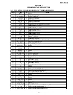
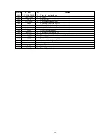
Pin No.
51
52
53
54
55
56
57
58
59
60
61
62
63
64
65
66
67
68
69
70
71
72
73
74
75
76
77
78
79
80
81
82
83
84
85
86
87
88
89
90
91
92
93
94
95
96
97
98
99
100
Pin Name
FLD_CS
LED_STB
_CE
AREA0
AREA1
IMUTE
FL_PCONT
TU_BST_C2
EEP_WP
EEP_SCL
EEP_SDA
EXT_PCONT
AREA2
BS_BIT_SW
BS_DECSW
BS_C_DET
BS_BOL_DET
BS_CONV_CONT
VCC
BS_BST_CONT
VSS
TU_PCONT
XNENTMUTE
DSEL
WIDE
S2SW
FR_PCONT
FSW
P_FAIL
AVLINK_IN_INT
KEY2_INT
KEY1_INT
EURO_MUTE
AUTO_PRESET
INSEL_PCONT
H_DET
SYNCRO_DET
INSEL1
INSEL2
INSEL_TU
FAN_SPEED
FAN_ONOFF
FAN_DET
IDET
XP_MUTE
KEY1
KEY2
KEY3
KEY4
KEY5
I/O
O
O
O
O
O
O
I
O
O
I/O
I
O
I
O
I
I
O
–
O
–
O
O
O
O
I
O
I
–
I
O
O
O
O
O
I
O
O
O
O
O
O
I
I
O
I
I
I
I
I
Function
Output of FLD driver chip select signal
Output of FLD driver storove signal
Fixed at “H”
Fixed at “H”
Not used
Output of FLD DC/DC converter power control signal
Not used
EEPROM writing protect signal input
Output of IIC clock signal with EEPROM
Input/output of IIC data signal with EEPROM
Fixed at “L”
Fixed at “L”
Not used
Not used
Not used
Not used
Not used
Power supply input (Analog 6V)
Not used
Digital GND
Tuner power supply control signal
Muting of S terminal/component signal output
D terminal output progressive / interlace switching
D terminal output aspect output signal (set to 4:3)
Detection of Line 2 S video signal
Output of FLD driver power control
Input of FALL power detection
AV LINK signal input
Not used
Not used
Not used
System reset signal
Output of video signal select
Detection of H sync signal
Output of sync detect
Output switching signal of Line 1
Output switching signal of Line 2
Output switching signal of tuner
Fan direction speed switching signal
Fan ON/OFF signal output
Detect of Fan stopping
Not used
Output muting signal of Audio
Input switching sigal of 1
Input switching sigal of 2
Input switching sigal of 3
Input switching sigal of 4
Digital GND
Summary of Contents for RDR-HX510
Page 6: ...MEMO 6 ...
Page 42: ...2 10E MEMO ...
Page 50: ...RDR HX510 MEMO 3 15 3 16E ...
Page 82: ...MEMO 5 4E ...

