FWD-32LX1R
3-6
3-10. FA1 Board
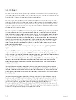
The FA1 board drives a fan for lowering the temperature in a unit. The fan has two- system control and its
speed can be controlled by modulating PWM of the fan drive signal from a microcomputer. A PWM
signal is amplified using an amplifier (IC5901) and then integrated and output in the later stage of Q5902
and Q5903 respectively. The fan voltage during shipping is fixed to 6.7 V for FAN (top) and 6.2 V for
FAN (left) when the unit is installed in the horizontal direction and 9.0 V for FAN (top) and 6.2 V for
FAN (left) when it is installed in the vertical direction.
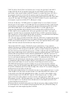
A fan detection signal (FAN_DET) is returned to the microcomputer via a fan detector (IC5900) because
a fan that outputs a fan operation detection signal is used. A maximum of eight fans can be connected. In
this unit, only three fans are connected. In this case, only the FAN_DET signal at pins 2, 5 and 14 of
CN5901 is used. A low-level signal (0 V) is output when normal operation is performed.
Since other detection ports of IC5900 are connected to GND, the output FAN_DET signal of IC5900
returns a high-level signal (3.3 V) to the microcomputer. The output FAN_DET signal of IC5900 returns
a low-level signal (0 V) when a fan is abnormal.
3-11. G4 Board
AC input/rectification block
CN7700 on the G4 board is connected to an AC inlet, and AC power is supplied from the AC inlet.
The input AC power is passed through an AC noise filter consisting of C7701, C7702, L7700, and L7701
and bridge-rectified by D7000.
Standby converter
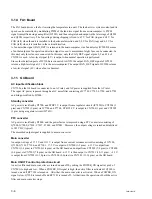
AC power is rectified by D7700, and STBY5 V is output from a regulator circuit (IC7420) to CN7204 (3
pins) and CN7205 (3 pins) via IC7700 and T7700. STBY3.3 V is output to CN7204 (1 pin) and CN7205
(1 pin) using a regulator circuit (IC7421).
PFC converter
AC power is rectified by D7000, and the power factor is improved using a PFC converter consisting of
Q7000, IC7000, C7014, C7017, L7001, and D7001. Moreover, the output voltage is raised and stabilized
to 385 VDC (typical).
The smoothed output signal is supplied to a main converter.
Main converter
An output voltage of 17.5 V and
±
13 V is output from a current resonance circuit consisting of IC7100,
Q7100, Q7101, T7100, and T7101. 17.5 V is output to CN7200 (1-5 pins).
+
13 V is output from
CN7201 (1-4 pins) to CN7500 (1-4 pins) on the GD board and output from CN7202 (7-8 pins) to CN7400
(3-4 pins) via CN7501 (7-8 pins) on the GD board.
+
13 V is then output to CN7203 (10-11 pins).
_
13 V
is output from CN7202 (13-14 pins) to CN7400 (8-9 pins) via CN7501 (13-14 pins) on the GD board.
Main ON/OFF control & protection circuit
An active filter and main converter are turned on and off by setting the POWER_ON signal (at pin 9 of
CN7203) to high and low. When a POWER_ON signal is high, the active filter is activated if Q7300 is
turned on and if RY7301 is turned on. After that, the main converter is activated. When a POWER_ON
signal is low, Q7300 is turned off and RY7301 is turned off. At that time, the operation of both the active
filter and main converter stops.
Summary of Contents for FWD-32LX1R Mounting Bracket
Page 6: ......
Page 26: ......
Page 42: ......
Page 50: ......
Page 52: ......
Page 94: ......
Page 124: ......
Page 126: ...9 2 FWD 32LX1R 9 2 D3 D3 1 A B C D 2 3 4 5 6 D3 A SIDE SUFFIX 11 ...
Page 127: ...9 3 FWD 32LX1R 9 3 D3 D3 1 A B C D 2 3 4 5 6 D3 B SIDE SUFFIX 11 ...
Page 129: ...9 5 FWD 32LX1R 9 5 1 A B C D E 2 3 4 5 6 7 8 G4 G4 G4 B SIDE SUFFIX 11 ...
Page 131: ...9 7 FWD 32LX1R 9 7 1 A B C 2 3 4 5 GD GD GD B SIDE SUFFIX 11 ...
Page 135: ...9 11 FWD 32LX1R 9 11 1 A B 2 3 4 5 K1 B SIDE SUFFIX 11 K1 K1 ...
Page 137: ...9 13 FWD 32LX1R 9 13 1 A B C 2 3 4 5 V1 V1 V1 B SIDE SUFFIX 11 ...
Page 139: ...9 15 FWD 32LX1R 9 15 1 A B 2 3 4 5 U1 B SIDE SUFFIX 11 U1 U1 ...
Page 142: ...Printed in Japan Sony Corporation 2006 4 22 2005 FWD 32LX1R SY E 9 878 393 02 ...


