background image

2-8

FWD-32LX1R

6.

Set an arbitrary target value by “Target Y Cont.” and
“Target Color”.

n

During factory setting, “Target Y Cont.” and “Target

Color” are adjusted by “2700”.

7.

Select “Auto Cal.” and press the 

[OK]

 key.

Automatic adjustment is started.
During adjustment, after the display becomes black &

white, it is colored again and the adjustment is
completed about ten seconds later.

8.

Select “AD Service Save” in the hierarchy of “AD
Calibration” and press the 

[OK]

 key.

The adjustment value is saved.

n

Save an adjustment value here.  Notice that the
adjustment value is not saved even if adjustment is

completed.

9.

After adjustment is completed, return the setting value
of “Adjust Picture” to the former value (value written

down in step 4) and exit the menu.

(2) Manual adjustment

S_VIDEO adjustment of OPTION1 slot
1.

Confirm that BKM-FW10 is installed in an OPTION1

slot.

2.

Select the S_VIDEO signal of OPTION1 by input

switching.

3.

Input a 75% color-bar signal to the S_VIDEO input

signal, selected in step 2, in an NTSC format and
display the screen.

4.

Start the service mode, select “Picture Mode” and then
“User1” by “Adjust Picture”, and set the items below.

n

After adjustment is completed, write down the setting

value before change so as t return the setting value of
“User1” to the former value.

Chroma:

50

Phase:

50

Noise Reduct.:

Off

Dynamic Picture:

Off

Color Correct:

Off

Gamma Correct:

Mid

5.

Select “AD Calibration”, “NTSC/PAL”, “Y/C Cal.”,
and then “Manual Control” in a service mode menu.

6.

Select “Adjust Y Contrast”. (Adjust the contrast.)

7.

Move a slider and adjust so that the “R”, “G”, and “B”
values displayed on the right of the slider are nearer

“2700” as far as possible.

8.

Select “Adjust C Level”. (Adjust the color.)

9.

Move a slider and adjust so that the “R” and “G”
values displayed on the right of the slider are nearer

“0” and so that the “B” value displayed on the right is
nearer “2700” as far as possible.

n

During factory setting, “Target Y Cont.” and “Target

Color” are adjusted by “2700”.

10. Select “AD Service Save” in the hierarchy of “AD

Calibration” and press the 

[OK]

 key.

The adjustment value is saved.

n

Save an adjustment value here.  Notice that the

adjustment value is not saved even if adjustment is
completed.

11. After adjustment is completed, return the setting value

of “Adjust Picture” to the former value (value written
down in step 4) and exit the menu.

3. AD calibration adjustment of video input signal

(SECAM signal)

(1) Automatic adjustment

Video adjustment of OPTION1 slot
1.

Confirm that BKM-FW10 is installed in an OPTION1

slot.

2.

Select the video signal of OPTION1 by input

switching.

3.

Input a 75% color-bar signal to the video input signal,

selected in step 2, in a SECAM format and display the
screen.

4.

Start the service mode, select “Picture Mode” and then
“User1” by “Adjust Picture”, and set the items below.

n

After adjustment is completed, write down the setting

value before change so as t return the setting value of
“User1” to the former value.

Chroma:

50

Phase:

50

Noise Reduct.:

Off

Dynamic Picture:

Off

Color Correct:

Off

Gamma Correct:

Mid

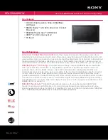
Summary of Contents for FWD-32LX1R Mounting Bracket

Page 1: ...FLAT PANEL DISPLAY FWD 32LX1R SERVICE MANUAL 1st Edition Revised 1 REMOTE COMMANDER RM 980 SPEAKER SYSTEM SS SP32FW TABLETOP STAND SU 32FW ...

Page 2: ...erden Um die Gefahr eines elektrischen Schlages Feuergefahr und Verletzungen zu vermeiden sind bei Wartungsarbeiten strikt die Angaben in der Anleitung zu befolgen Andere als die angegeben Wartungsarbeiten dürfen nur von Personen ausgeführt werden die eine spezielle Befähigung dazu besitzen AVERTISSEMENT Ce manual est destiné uniquement aux personnes compétentes en charge de l entretien Afin de ré...

Page 3: ...arattillverkaren Kassera använt batteri enligt gällande föreskrifter VAROITUS Paristo voi räjähtää jos se on virheellisesti asennettu Vaihda paristo ainoastaan laitevalmistajan suosittelemaan tyyppiin Hävitä käytetty paristo valmistajan ohjeiden mukaisesti CAUTION Danger of explosion if battery is incorrectly replaced Replace only with the same or equivalent type recommended by the manufacturer Di...

Page 4: ...ubstitute items the Display Unit may fall and cause bodily injury to someone or damage to the Display Unit Be sure to assemble the bracket properly following the instructed procedure explained in the instruction manual of the Wall Mount Bracket Be sure to tighten the screws securely in the designated position If you fail to do so the Display Unit may fall and cause bodily injury to someone or dama...

Page 5: ...ay When you set up the Display Unit make sure there is more space around the display than that shown in the figure below This will allow for proper ventilation Wile the unit is on a certain amount of heat builds up inside This can cause burns Avoid touching the top or rear of the unit when it is powered on or just after it has entered standby mode When mounting the display horizontally When mounti...

Page 6: ......

Page 7: ...D3 Board V1 Board 1 5 1 4 2 FA1 Board GD Board 1 6 1 4 3 G4 Board 1 7 1 4 4 K1 Board 1 8 1 4 5 S Board 1 8 1 4 6 H1 Board 1 9 1 4 7 H2 Board 1 9 1 4 8 H3 Board 1 10 1 4 9 SP Board 1 10 1 4 10 U1 Board 1 11 1 5 Replacing the Main Parts 1 11 1 5 1 DC Fan 1 11 1 5 2 Lithium Battery 1 12 1 5 3 LCD Module 1 13 1 6 Service Position 1 14 1 6 1 Service Position of D3 Board FA1 Board G4 Board GD Board K1 B...

Page 8: ...Diagrams D3 8 2 FA1 8 11 G4 8 12 GD 8 14 H1 8 16 H2 8 16 H3 8 16 S 8 16 SP 8 16 K1 8 17 U1 8 19 V1 8 20 Frame Wiring 8 29 9 Board Layouts D3 9 1 G4 9 4 GD 9 6 FA1 9 8 H1 9 9 H2 9 9 H3 9 9 K1 9 10 V1 9 12 U1 9 14 S 9 16 SP 9 16 ...

Page 9: ...LX1R Section 1 Service Overview 1 1 Appearance Figure 1 2 Board Location 1 2 3 4 5 6 7 8 9 0 ON SET OFF H3 board H2 board H1 board FA1 board K1 board G4 board GD board D3 board V1 board U1 board S board SP board ...

Page 10: ...ide and loosen the two panel securing screws then remove the U1 block assembly 2 Remove the four screws PSW M6 x 20 then remove the four knobs 3 Remove the seven screws PSW4 x 12 then hold the two handles and remove the cabinet assembly Installation 4 Reattach the cabinet assembly in the reverse order of steps 1 to 3 PSW M6 x 20 PSW 4 x 12 Knobs Cabinet assembly U1 block assembly Panel securing sc...

Page 11: ...s from the connector CN9200 on the H2 board 3 Disconnect the harness from the connector CN9300 on the H3 board 4 Remove the twelve screws then hold the four portions A and remove the chassis assembly Installation 5 Reattach the chassis assembly in the reverse order of steps 2 to 4 6 Reattach the cabinet assembly Refer to Section 1 3 1 Harnesses Bezel assembly H3 board H2 board Chassis assembly Por...

Page 12: ...en remove the shield cover G Installation 4 Reattach the shield cover G and two arms in the reverse order of steps 2 and 3 n When attaching the two arms be careful of the orientation of the imprinting 5 Reattach the cabinet assembly Refer to Section 1 3 1 BVTT 4 x 8 BVST 4 x 8 BVST 3 x 6 BVST 3 x 6 Arm Shield cover G Connector Arm Imprinting L Base chassis assembly Conductive cushion DC fan Imprin...

Page 13: ... D3 board 6 Disconnect the four harnesses from the connectors CN3901 CN3904 on the V1 board 7 Remove the nine screws BVST3 x 6 then remove the D3 and V1 boards 8 Remove the hexagonal screw BVTP3 x 12 then remove the connector panel assembly 9 Remove the V1 board from the connector CN1000 on the D3 board in the direction of the arrow A BVTP 3 x 12 BVST 3 x 6 BVST 3 x 6 BVST 3 x 6 BVST 3 x 6 Harness...

Page 14: ...Section 1 4 3 Disconnect the three harnesses from the connectors CN5900 CN5902 on the FA1 board 4 Remove the four screws then remove the FA1 board 5 Disconnect the eight harnesses from the connectors CN7400 CN7405 CN7500 and CN7501 on the GD board 6 Remove the four screws then remove the GD board Installation 7 Install the FA1 board and GD board in the reverse order of steps 3 to 6 8 Reassemble th...

Page 15: ...from the connectors CN7200 CN7205 CN7700 on the G4 board 4 Remove the six screws 5 Remove the G4 board from the two locking card spacers Installation 6 Install the G4 board in the reverse order of steps 3 to 5 7 Reassemble this unit in the reverse order of steps 1 and 2 Harnesses Harness G4 board G4 board Locking card spacer Conductive cushion CN7205 CN7700 CN7204 CN7203 CN7201 CN7202 CN7200 BVST ...

Page 16: ...ssemble this unit in the reverse order of steps 1 and 2 1 4 5 S Board Removal 1 Remove the cabinet assembly Refer to Section 1 3 1 2 Remove the shield cover G and two arms Refer to steps 2 and 3 of Section 1 4 3 Disconnect the harness from the connector CN9400 on the S board 4 Remove the screw then remove the S board Installation 5 Install the S board in the reverse order of steps 3 and 4 6 Reasse...

Page 17: ...n 1 3 1 2 Remove the bezel assembly Refer to Section 1 3 2 3 Remove the hook from the rib in the center of the lower portion on the bezel assembly 4 Slowly incline the H2 board in the direction of the arrow then remove it from the bezel assembly Installation 5 Install the H2 board n When installing the H2 board insert the two hooks upper portion into the openings of the cabinet assembly and push i...

Page 18: ...cord 5 Reattach the cabinet assembly Refer to Section 1 3 1 1 4 9 SP Board Removal 1 Remove the cabinet assembly Refer to Section 1 3 1 2 Remove the shield cover G and two arms Refer to steps 2 and 3 of Section 1 4 3 Disconnect the harness from the connector CN9500 on the SP board 4 Remove the two screws then remove the SP board Installation 5 Install the SP board in the reverse order of steps 3 a...

Page 19: ...careful of the orientation of the imprinting If the power is turned on with the DC fan removed state the self diagnosis function Section 4 2 is activated DC fan left Removal 1 Remove the cabinet assembly Refer to Section 1 3 1 2 Disconnect the connector and remove the two screws BVST3 x 6 then remove the fan bracket G 3 Remove the two screws PSW3 x 12 then remove the DC fan Installation 4 Reattach...

Page 20: ...2 Battery holder Lithium battery D3 board Conductive cushion DC fan top Removal 1 Remove the cabinet assembly Refer to Section 1 3 1 2 Remove the shield cover G and two arms Refer to steps 2 and 3 of Section 1 4 3 Disconnect the two connectors and remove the two screws BVST3 x 6 then remove the fan bracket top assembly 4 Remove the four screws PSW3 x 12 then remove the two DC fans Installation 5 R...

Page 21: ... Adjustment Removal 1 Remove the cabinet assembly Refer to Section 1 3 1 2 Remove the bezel assembly Refer to Section 1 3 2 3 Remove the two arms and shield cover G Refer to Section 1 4 4 Remove the DC fan top Refer to Section 1 5 1 5 Remove the D3 board V1 board and G4 board Refer to Sections 1 4 1 and 1 4 3 6 Remove the four screws PS5 x 10 and disconnect the two harness then remove the base cha...

Page 22: ...3 of Section 1 4 3 Reattach the two arms removed in step 2 with eight screws 4 Reattach the four knobs to this unit removed in step 1 with four screws 5 Insert the four knobs into the holes of the two stands 1 6 Service Position 1 6 1 Service Position of D3 Board FA1 Board G4 Board GD Board K1 Board V1 Board m When attaching this unit to the stands be sure to work with two persons After attaching ...

Page 23: ...t follow the instruction provided separately 2 Capron sheet 9 Carton 8 Individual packing carton When sending one or two individual packing cartons put the dummy box 7 Lid 4 LCD module 3 Individual packing carton 1 LCD module The glass surface must the capron sheet 6 Cushions B 5 Cushions A ...

Page 24: ...to be applied to the solder joint for a slightly longer time The printed pattern copper foil may peel away if the heated tip is applied for too long so be careful 1 8 Replacing the Battery The lithium battery for clock is mounted on the D3 board c When replacing the part be sure to use the specified one below Replacement with a part other than the specified part will result in fire hazards and ele...

Page 25: ...nd Australia Japan Canada New Zealand Plug type VM0233 COX 07 636 1 VM1296 Female end VM0089 COX 02 VM0310B VM0303B VM1313 Cord type SVT H05VV F CEE 13 53rd O C HVCTF Minimum cord 10 A 125 V 10 A 250 V 10 A 250 V 10 A 125 V set rating Safety approval UL CSA VDE VDE DENAN HO 1 Use an appropriate rating plug which complies with local regulations ...

Page 26: ......

Page 27: ...r electric adjustment Start To enter the service mode using RM 980 press the DISPLAY 5 VOL and POWER ON keys sequentially with this unit put into the standby state Cancellation To cancel the service mode put the unit into the standby state again using a STBY key or turn off the power Viewing the screen 1 Change in Picture Mode Refer to Section 2 2 2 2 Picture quality adjustment Refer to Section 2 ...

Page 28: ...s unit Select DVI for input switching 3 Start the service mode select Picture Mode and then User1 by Adjust Picture and set the items below n After adjustment is completed write down the setting value before change so as to return the setting value of User1 to the former value Backlight 50 Contrast 50 Brightness 75 Chroma 50 Phase 50 Noise Reduct Off Dynamic Picture Off Color Correct Off Gamma Cor...

Page 29: ...e Warm 13 Perform the adjustment in steps 5 to 9 14 After adjustment is completed return the setting value of Adjust Picture to the former value value written down in step 3 and exit the menu 2 2 7 AD Calibration Adjustment This unit has one slot OPTION1 Install BKM FW10 FW11 in the slot to be adjusted as required n To correctly adjust the AD calibration perform aging in the aging mode for 30 minu...

Page 30: ...ent Setting range 2 000 to 4 000 Manual Control Menu configuration NTSC PAL Composite Cal Manual Control Y Contrast Adjusts the Y level Adjustment range 0 to 255 C Level Adjusts the C level Adjustment range 0 to 255 Composite Cal Y C Cal SECAM Adjusts the calibration of SECAM signal SECAM Composite Cal Adjusts the Composite signal Y C Cal Adjusts the Y C signal Composite Cal Menu configuration SEC...

Page 31: ...R Offset 128 G Offset 128 B Offset 128 Manual Control Menu configuration Analog RGB RGB Cal Manual Control R Gain Adjusts the red gain Adjustment range 0 to 255 G Gain Adjusts the green gain Adjustment range 0 to 255 B Gain Adjusts the blue gain Adjustment range 0 to 255 R Offset Adjusts the red offset Adjustment range 0 to 255 G Offset Adjusts the green offset Adjustment range 0 to 255 B Offset A...

Page 32: ...n below 75 indicates that the level in a white zone is 75 IRE Video adjustment of OPTION1 slot 1 Confirm that BKM FW10 is installed in an OPTION1 slot 2 Select the video signal of OPTION1 by input switching 3 Input a 75 color bar signal to the video input signal selected in step 2 in an NTSC format and display the screen 4 Start the service mode select Picture Mode and then User1 by Adjust Picture...

Page 33: ...and adjust so that the R G and B values displayed on the right of the slider are nearer 2700 as far as possible 8 Select Adjust C Level Adjust the color 9 Move a slider and adjust so that the R and G values displayed on the right of the slider are nearer 0 and so that the B value displayed on the right is nearer 2700 as far as possible n During factory setting Target Y Cont and Target Color are ad...

Page 34: ... Y C Cal and then Manual Control in a service mode menu 6 Select Adjust Y Contrast Adjust the contrast 7 Move a slider and adjust so that the R G and B values displayed on the right of the slider are nearer 2700 as far as possible 8 Select Adjust C Level Adjust the color 9 Move a slider and adjust so that the R and G values displayed on the right of the slider are nearer 0 and so that the B value ...

Page 35: ...elect AD Calibration SECAM Composite Cal and then Manual Control in a service mode menu 6 Select Adjust Y Contrast Adjust the contrast 7 Move a slider and adjust so that the R G and B values displayed on the right of the slider are nearer 2700 as far as possible 8 Select Adjust C Level Adjust the color 9 Move a slider and adjust so that the R and G values displayed on the right of the slider are n...

Page 36: ...ual Control in a service mode menu 6 Select Adjust Y Contrast Adjust the contrast 7 Move a slider and adjust so that the R G and B values displayed on the right of the slider are nearer 2700 as far as possible 8 Select Adjust C Level Adjust the color 9 Move a slider and adjust so that the R and G values displayed on the right of the slider are nearer 0 and so that the B value displayed on the righ...

Page 37: ...value value written down in steps 3 and 11 and exit the menu 2 Manual adjustment CCP2 Component adjustment of INPUT2 terminal 1 Select the component signal of INPUT2 by input switching 2 Input a 75 color bar signal to the component input signal selected in step 1 in a 720 60P format and display the screen 3 Start the service mode select Picture Mode and then User1 by Adjust Picture and set the ite...

Page 38: ...press the OK key Automatic adjustment is started When adjustment is completed ADC Finished is displayed in the center of the screen 6 Select AD Service Save in the hierarchy of AD Calibration and press the OK key The adjustment value is saved n Save an adjustment value here Notice that the adjustment value is not saved even if adjustment is completed Component adjustment of OPTION1 slot 7 Confirm ...

Page 39: ...c signal and display the screen 21 Execute steps 3 to 18 22 After adjustment is completed return the setting value of Adjust Picture to the former value value written down in steps 3 and 21 and exit the menu 6 AD calibration adjustment of analog RGB input signal 1 Automatic adjustment RGB adjustment of INPUT2 terminal 1 Select the RGB signal of INPUT2 by input switching 2 Input a 100 color bar sig...

Page 40: ...nearer 4000 as far as possible 11 Select Adjust R Offset 12 Move a slider and adjust it to the value on whether R value 1 of information display changes to the upper position 13 Select Adjust G Offset 14 Move a slider and adjust it to the value on whether B value 1 of information display changes to the upper position 15 Select Adjust B Offset 16 Move a slider and adjust it to the value on whether ...

Page 41: ...0 5 seconds After aging continuously passes for 30 minutes the LED indicator blinks in green at intervals of three seconds After the current mode is shifted to the aging mode keys other than the standby button are invalidated The way to cancel the aging mode after it is shifted is as described below Turn on and off the standby and AC state Input a signal to the current input signal V Slice Control...

Page 42: ......

Page 43: ...r making the logo of Sony bright H3 board For detail refer to Section 3 6 The H3 board has the photosensing block of remote commander and two color LED that indicate the state of this unit K1 board For detail refer to Section 3 7 The K1 board is an audio signal processing board It has a surround processor IC and power amplifier IC SP board For detail refer to Section 3 8 The SP board has a speaker...

Page 44: ...r as an eight bit digital RGB signal In a scaler IC2300 resolution is converted according to the resolution of a display panel Also a wide angle or zoom function is set as required A TMDS receiver is mounted for the input signal from an INPUT1 terminal A D converter is mounted in an analog input port Three input ports including a video port are provided This enables the two screen display of P P a...

Page 45: ...ter and scaler can be rewritten By using an interface IC1002 the signal of an RS 232C connector is output to this unit in the range of 5 V and to the external connection unit in the range of 12 V IC1002 is connected with a microcomputer and scaler using a communication selector switch IC1004 and can be communicated using UART External communication can be performed from the network board BKM FW32 ...

Page 46: ...ted using an RGB switch IC3001 and then output from CN3900 to the D3 board The signal input to the video switch is output to a SECAM decoder IC3300 and NTSC PAL decoder IC3505 The SECAM decoder IC3300 separates a SECAM signal from Y to C and converts it from analog to digital The NTSC PAL decoder IC3505 separates signals other than a SECAM signal from Y to C and converts them from analog to digita...

Page 47: ...pplying 3 3 V to an anode and controlling a cathode 3 7 K1 Board Input audio signals AU_L and AU_R are input from the D3 board to a surround processor IC5000 through CN5000 In the surround processor the volume balance bass and treble are controlled and the hall simulation of surrounding is processed After that audio L and R signals are input to class D power amplifiers IC5001 and IC5002 and PWM mo...

Page 48: ...ed through an AC noise filter consisting of C7701 C7702 L7700 and L7701 and bridge rectified by D7000 Standby converter AC power is rectified by D7700 and STBY5 V is output from a regulator circuit IC7420 to CN7204 3 pins and CN7205 3 pins via IC7700 and T7700 STBY3 3 V is output to CN7204 1 pin and CN7205 1 pin using a regulator circuit IC7421 PFC converter AC power is rectified by D7000 and the ...

Page 49: ...ins and CN7401 The DC DC converter is turned on and off by setting the POWER_ON signal CN7203 pin 9 on the G4 board CN7202 pin 3 and CN7501 pin 3 on the GD board and PON PANEL signal at pin 7 of CN6404 from a microcomputer to high and low A high level signal is first input from CN7501 3 pins POWER_ON signal to IC7500 9 10 pins and IC7600 10 pins and A5 V A3 3 V and D3 3 V are output After two seco...

Page 50: ......

Page 51: ... power is turned on POWER STANDBY indicator Front side 2 Increase in sensor temperature This detects the temperature of the S board and power supply boards G4 and GD boards This unit shuts down when the state in which the temperatures below were exceeded is detected for two seconds or more Installed Power Installed Power horizontally supply vertically supply S board board S board board 55dC 82dC 6...

Page 52: ......

Page 53: ... DC001 03 HN1D03FU TE85L DC005 05 HN1D03FU TE85R DC005 05 M1FS4 4063 DC008 02 MA113 TX DC008 01 MA2S111 K8 DC008 01 MA3130WA TX DC001 18 NSQ03A06 TE16L DC007 01 PTZ TE25 6 8B DC008 04 RB060L 40TE25 DC007 01 RB551V 30TE 17 DC008 02 UDZS TE17 5 6B DC008 04 UDZS TE17 9 1B DC008 04 UDZSTE 173 6B DC008 04 TRANSISTOR Page or ID No 2SA1037AK T146 R TC001 01 2SA1226 E4 TC001 01 2SA1226 T1E3E4 TC001 01 2SA...

Page 54: ... E2 SN74LV125APWR MC74HC125N SN74LV4053APWR MC74HC4053F TA78M09F TE16L TA78M09F TC74HC123AF TC74HC123P TC74LCX00FT EL TC74HC00P TC74LCX125FT EL MC74HC125N TC74LCX14F EL TC74HC14P TC74LCX244FT EL TC74HC244P TC74VHC86FT EL TC74HC86P TC74VHCT125AFT EL MC74HC125N TC7SZ125FU TE85R NC7SZ125P5 TC7SZ126FU TE85R NC7SZ126P5 TC7W04FU TE12R TC7W04F TC7W04FU TC7W04F THC63LVDM83R T THC63LVDM83A T TLC2933IPWR 12...

Page 55: ...ndardization of Parts Some repair parts supplied by Sony differ from those used for the unit These are because of parts common ality and improvement Parts list has the present standardized repair parts 3 Stock of Parts Parts marked with o at SP Supply Code column of the spare parts list may not be stocked Therefore the delivery date will be delayed 4 Harness Harnesses with no part number are not r...

Page 56: ...ock 6 2 Exploded Views B C C E D F F A E D A B PSW M6 x 20 BVTP 3 x 8 BVTP 3 x 8 BVTP 3 x 12 4 18 22 22 22 22 22 22 22 22 23 22 20 22 22 22 22 23 7 1 11 21 22 22 15 16 16 24 27 5 2 3 8 6 9 10 17 12 28 13 14 14 14 18 25 19 26 ...

Page 57: ... 11 X 2023 396 7 s CABINET ASSY 12 1 251 382 21 s INLET AC 3P WITH NOISE FILTE 13 1 756 157 11 s BATTERY LITHIUM 14 1 763 659 11 s FAN DC 15 2 159 508 01 s CABLE COVER BOTTOM 16 2 179 449 01 s CABLE COVER SIDE 17 2 580 593 01 s SCREW PSW M3X8 18 2 580 594 01 s SCREW PSW M3X12 19 2 580 598 01 s SCREW PSW M3X30 20 2 580 600 01 s SCREW PSW M4X8 21 2 580 602 01 s SCREW PSW M4X12 22 2 580 628 01 s SCRE...

Page 58: ...6 4 FWD 32LX1R Chassis Block A A B B PS 5 x 10 BVTP 3 x 8 105 112 112 114 114 113 114 113 114 109 110 102 103 101 104 106 117 117 117 107 115 116 108 111 ...

Page 59: ...SY BLACK 105 X 2102 876 1 s COVER ASSY LVDS 106 1 805 870 21 s LCD PANEL 32INCH WXGA TFT 107 1 831 405 11 s LEAD WIRE WITH CONNECTOR 108 2 159 493 02 s LIGHT GUIDE 109 2 548 276 02 s PANEL BUTTON CONTROL 110 2 548 277 01 s BUTTON CONTROL 111 2 580 594 01 s SCREW PSW M3X12 112 2 580 628 01 s SCREW BVST 3X6 113 2 580 630 01 s SCREW BVST 4X8 114 2 580 639 01 s SCREW BVTP2 4X12 115 4 052 842 01 s HOLD...

Page 60: ... 32R RP FOR SS SP32FW W PEARL WHITE 202 A 1081 106 A s SPEAKER ASSY 32L RP FOR SS SP32FW S SILVER A 1083 768 A s SPEAKER ASSY 32L RP FOR SS SP32FW W PEARL WHITE 7 682 962 09 s SCREW PSW 4X10 7 685 661 79 s SCREW BVTP4X12 EP FE ZNBK CM2 Overall SS SP32FW BVTP 4 x 12 BVTP 4 x 12 BVTP 4 x 12 BVTP 4 x 12 PSW 4 x 10 PSW 4 x 10 201 202 ...

Page 61: ...6 7 FWD 32LX1R Overall SU 32FW No Part No SP Description 301 2 560 385 01 o COVER REAR SUPPORT 301 ...

Page 62: ...APACITOR CERAMIC 10PF 50V CH C1234 1 162 974 11 s CAPACITOR CERAMIC 0 01MF 50V F C1235 1 107 826 11 s CAPACITOR CHIP CERAMIC 0 1MF C1236 1 125 837 91 s CAPACITOR CHIP CERAMIC1MF 6 3V D3 BOARD Ref No or Q ty Part No SP Description C1237 1 107 826 11 s CAPACITOR CHIP CERAMIC 0 1MF C1238 1 107 826 11 s CAPACITOR CHIP CERAMIC 0 1MF C1239 1 115 156 11 s CAPACITOR CERAMIC 1MF 10V 1608 C1240 1 107 826 11...

Page 63: ...C1836 1 162 927 11 s CAPACITOR CERAMIC 100PF 50V CH C1837 1 107 826 11 s CAPACITOR CHIP CERAMIC 0 1MF D3 BOARD Ref No or Q ty Part No SP Description C1838 1 125 777 11 s CAPACITOR CERAMIC 0 1MF 10V C1841 1 162 964 11 s CAPACITOR CERAMIC 1000PF 50V B C1842 1 125 837 91 s CAPACITOR CHIP CERAMIC1MF 6 3V C1843 1 127 760 11 s CAPACITOR CERAMIC 4 7MF 6 3V C2000 1 165 811 11 s CAPACITOR CHIP CERAMIC 22MF...

Page 64: ...05 1 125 777 11 s CAPACITOR CERAMIC 0 1MF 10V C2306 1 125 777 11 s CAPACITOR CERAMIC 0 1MF 10V C2307 1 125 777 11 s CAPACITOR CERAMIC 0 1MF 10V D3 BOARD Ref No or Q ty Part No SP Description C2308 1 125 777 11 s CAPACITOR CERAMIC 0 1MF 10V C2309 1 125 777 11 s CAPACITOR CERAMIC 0 1MF 10V C2310 1 125 777 11 s CAPACITOR CERAMIC 0 1MF 10V C2311 1 125 777 11 s CAPACITOR CERAMIC 0 1MF 10V C2312 1 125 7...

Page 65: ... CONNECTOR BOARD TO BOARD 100P CN1001 1 564 507 11 o PLUG CONNECTOR 4P CN1002 1 564 516 11 o PLUG CONNECTOR 13P CN1003 1 564 515 11 o PLUG CONNECTOR 12P CN1004 1 564 595 11 o PLUG CONNECTOR 14P CN1005 1 564 509 11 o PLUG CONNECTOR 6P CN1006 1 565 269 31 s SOCKET CONNECTOR D DUB L 9P CN1007 1 764 078 11 s PIN CONNECTOR PC BOARD 3P CN1008 1 564 510 11 o PLUG CONNECTOR 7P D3 BOARD Ref No or Q ty Part...

Page 66: ...O CHIP TYPE FB2002 1 414 445 11 s FERRITE EMI SMD D3 BOARD Ref No or Q ty Part No SP Description FB2003 1 500 451 11 s MICRO INDUCTOR CHIP 41P750S FB2004 1 500 451 11 s MICRO INDUCTOR CHIP 41P750S FB2200 1 414 445 11 s FERRITE EMI SMD FB2201 1 414 445 11 s FERRITE EMI SMD FB2202 1 414 864 11 s INDUCTOR MICRO CHIP TYPE FB2203 1 414 864 11 s INDUCTOR MICRO CHIP TYPE FB2300 1 469 100 21 s FERRITE EMI...

Page 67: ...TK H04 Q1009 8 729 905 35 s TRANSISTOR 2SC4081 R Q1010 8 729 029 14 s TRANSISTOR DTC144EUA T106 Q1201 8 729 028 96 s TRANSISTOR DTC114EUA T106 Q1204 8 729 028 96 s TRANSISTOR DTC114EUA T106 Q1209 8 729 901 81 s TRANSISTOR 2SC2412K T 146 R Q1210 6 550 014 01 s TRANSISTOR SSM6N15FU TE85R Q1211 8 729 901 81 s TRANSISTOR 2SC2412K T 146 R Q1212 6 550 014 01 s TRANSISTOR SSM6N15FU TE85R Q1214 8 729 901 ...

Page 68: ...TOR CHIP 1608 R1226 1 216 864 11 s CONDUCTOR CHIP 1608 R1227 1 216 864 11 s CONDUCTOR CHIP 1608 D3 BOARD Ref No or Q ty Part No SP Description R1231 1 216 864 11 s CONDUCTOR CHIP 1608 R1233 1 216 809 11 s RESISTOR CHIP 100 1 10W 1608 R1234 1 216 809 11 s RESISTOR CHIP 100 1 10W 1608 R1238 1 216 841 11 s RESISTOR CHIP 47K 1 10W 1608 R1240 1 216 864 11 s CONDUCTOR CHIP 1608 R1248 1 216 864 11 s COND...

Page 69: ... CHIP 1 0K 1 10W 1608 R1383 1 216 849 11 s RESISTOR CHIP 220K 1 16W 1608 D3 BOARD Ref No or Q ty Part No SP Description R1384 1 216 833 11 s RESISTOR CHIP 10K 1 10W 1608 R1385 1 216 845 11 s RESISTOR CHIP 100K 1 10W 1608 R1387 1 216 864 11 s CONDUCTOR CHIP 1608 R1391 1 216 864 11 s CONDUCTOR CHIP 1608 R1395 1 216 809 11 s RESISTOR CHIP 100 1 10W 1608 R1397 1 216 809 11 s RESISTOR CHIP 100 1 10W 16...

Page 70: ...649 1 216 805 11 s RESISTOR CHIP 47 1 10W 1608 R1658 1 216 801 11 s RESISTOR CHIP 22 1 10W 1608 R1661 1 216 801 11 s RESISTOR CHIP 22 1 10W 1608 D3 BOARD Ref No or Q ty Part No SP Description R1662 1 216 801 11 s RESISTOR CHIP 22 1 10W 1608 R1663 1 216 853 11 s RESISTOR CHIP 470K 1 16W 1608 R1664 1 216 825 11 s RESISTOR CHIP 2 2K 1 10W 1608 R1665 1 216 825 11 s RESISTOR CHIP 2 2K 1 10W 1608 R1666 ...

Page 71: ...SISTOR CHIP 220K 1 16W 1608 R1881 1 216 849 11 s RESISTOR CHIP 220K 1 16W 1608 R1882 1 216 809 11 s RESISTOR CHIP 100 1 10W 1608 R1883 1 216 821 11 s RESISTOR CHIP 1 0K 1 10W 1608 D3 BOARD Ref No or Q ty Part No SP Description R1884 1 216 864 11 s CONDUCTOR CHIP 1608 R1885 1 216 857 11 s RESISTOR CHIP 1M 1 10W 1608 R1886 1 216 833 11 s RESISTOR CHIP 10K 1 10W 1608 R1887 1 216 805 11 s RESISTOR CHI...

Page 72: ...TOR CHIP 22 1 16W 1005 R2409 1 208 643 11 s RESISTOR CHIP 22 1 16W 1005 R2410 1 208 643 11 s RESISTOR CHIP 22 1 16W 1005 D3 BOARD Ref No or Q ty Part No SP Description R2411 1 218 871 11 s RESISTOR CHIP 10K 1 10W 1608 R2412 1 218 871 11 s RESISTOR CHIP 10K 1 10W 1608 R2413 1 218 827 11 s RESISTOR CHIP 150 1 10W 1608 R2414 1 218 851 11 s RESISTOR CHIP 1 5K 1 10W 1608 R2416 1 216 809 11 s RESISTOR C...

Page 73: ...K 100X4 1005 RB1218 1 239 388 11 s NETWORK RESISTOR CHIP 68 RB1219 1 234 372 11 s RES NETWORK 100X4 1005 RB1220 1 234 372 11 s RES NETWORK 100X4 1005 D3 BOARD Ref No or Q ty Part No SP Description RB1221 1 234 372 11 s RES NETWORK 100X4 1005 RB1222 1 234 372 11 s RES NETWORK 100X4 1005 RB1223 1 234 370 11 s RES NETWORK 22X4 1005 RB1224 1 234 372 11 s RES NETWORK 100X4 1005 RB1225 1 234 372 11 s RE...

Page 74: ...C 0 1MF 50V C5916 1 117 681 11 s CAPACITOR ELECT 100MF 16V C5917 1 126 204 11 s CAPACITOR ELECT 47MF 16V CHIP C5918 1 107 826 11 s CAPACITOR CHIP CERAMIC 0 1MF C5919 1 117 681 11 s CAPACITOR ELECT 100MF 16V C5920 1 115 339 11 s CAPACITOR CERAMIC 0 1MF 50V C5921 1 115 339 11 s CAPACITOR CERAMIC 0 1MF 50V C5922 1 117 681 11 s CAPACITOR ELECT 100MF 16V CN5900 1 564 510 11 o PLUG CONNECTOR 7P CN5901 1...

Page 75: ... 1 137 807 11 s CAPACITOR ELECT 100MF 50V C7020 1 107 910 11 s CAPACITOR ELECT 100MF 50V C7100 1 162 970 11 s CAPACITOR CERAMIC 0 01MF 25V B C7101 1 107 905 11 s CAPACITOR ELECT 4 7MF 50V C7102 1 107 909 11 s CAPACITOR ELECT 47MF 50V C7103 1 162 970 11 s CAPACITOR CERAMIC 0 01MF 25V B C7104 1 100 831 91 s CAP CHIP CERAMIC 1000PF CH1608 C7105 1 107 906 11 s CAPACITOR ELECT 10MF 50V 105 C7107 1 162 ...

Page 76: ...202 8 719 060 88 s DIODE D4SBS6 D7203 8 719 060 88 s DIODE D4SBS6 D7300 8 719 948 45 s DIODE ERA22 08 D7301 8 719 074 43 s DIODE BAS316 115 D7302 8 719 074 43 s DIODE BAS316 115 D7303 8 719 074 43 s DIODE BAS316 115 G4 BOARD Ref No or Q ty Part No SP Description D7304 8 719 074 43 s DIODE BAS316 115 D7305 8 719 083 70 s DIODE UDZSTE 1727B D7306 8 719 074 43 s DIODE BAS316 115 D7307 8 719 977 28 s ...

Page 77: ...DUCTOR CHIP 1608 R7200 1 216 825 11 s RESISTOR CHIP 2 2K 1 10W 1608 G4 BOARD Ref No or Q ty Part No SP Description R7201 1 216 821 11 s RESISTOR CHIP 1 0K 1 10W 1608 R7202 1 216 864 11 s CONDUCTOR CHIP 1608 R7203 1 216 833 11 s RESISTOR CHIP 10K 1 10W 1608 R7204 1 216 864 11 s CONDUCTOR CHIP 1608 R7205 1 218 876 11 s RESISTOR CHIP 16K 1 10W 1608 R7207 1 218 857 11 s RESISTOR CHIP 2 7K 1 10W 1608 R...

Page 78: ... 1 128 528 11 s CAPACITOR ELECT 470MF 25V C7501 1 100 118 21 s CAPACITOR ELECT 82MF 16V 8X7 C7502 1 162 970 11 s CAPACITOR CERAMIC 0 01MF 25V B C7503 1 162 970 11 s CAPACITOR CERAMIC 0 01MF 25V B C7504 1 162 970 11 s CAPACITOR CERAMIC 0 01MF 25V B C7505 1 162 923 11 s CAPACITOR CERAMIC 47PF 50V CH C7506 1 125 779 21 s CAP CERAMIC 0 022MF B 1608 C7507 1 164 004 11 s CAPACITOR CERAMIC 0 1MF 25V C750...

Page 79: ...0K 1 10W 1608 R7419 1 216 833 11 s RESISTOR CHIP 10K 1 10W 1608 R7500 1 218 871 11 s RESISTOR CHIP 10K 1 10W 1608 R7501 1 218 871 11 s RESISTOR CHIP 10K 1 10W 1608 R7502 1 216 841 11 s RESISTOR CHIP 47K 1 10W 1608 GD BOARD Ref No or Q ty Part No SP Description R7503 1 216 841 11 s RESISTOR CHIP 47K 1 10W 1608 R7504 1 218 843 11 s RESISTOR CHIP 680 1 10W 1608 R7505 1 216 821 11 s RESISTOR CHIP 1 0K...

Page 80: ...829 11 s SWITCH TACTILE S9104 1 692 829 11 s SWITCH TACTILE S9105 1 692 829 11 s SWITCH TACTILE H2 BOARD Ref No or Q ty Part No SP Description CN9200 1 573 806 21 s PIN CONNECTOR 6P SMD 1 5MM D9203 6 500 012 61 s DIODE NSCW215T A1A2ST D9204 6 500 012 61 s DIODE NSCW215T A1A2ST R9200 1 216 864 11 s CONDUCTOR CHIP 1608 R9201 1 216 864 11 s CONDUCTOR CHIP 1608 R9202 1 216 864 11 s CONDUCTOR CHIP 1608...

Page 81: ...s CAPACITOR CERAMIC 1MF 25V C5051 1 163 021 91 s CAPACITOR CERAMIC 0 01MF 50V C5052 1 125 827 11 s CAPACITOR CERAMIC 1MF 25V C5053 1 125 827 11 s CAPACITOR CERAMIC 1MF 25V C5054 1 126 395 11 s CAPACITOR ELECT 22MF 16V CHIP C5055 1 137 980 91 s CAPACITOR CHIP CERAMIC 0 47MF C5056 1 137 980 91 s CAPACITOR CHIP CERAMIC 0 47MF K1 BOARD Ref No or Q ty Part No SP Description C5057 1 127 573 11 s CAPACIT...

Page 82: ... CAP ELECT 47MF 10V C6 1 127 573 11 s CAPACITOR CERAMIC 1MFB 2012 C7 1 162 970 11 s CAPACITOR CERAMIC 0 01MF 25V B C8 1 162 970 11 s CAPACITOR CERAMIC 0 01MF 25V B C10 1 162 970 11 s CAPACITOR CERAMIC 0 01MF 25V B C12 1 162 970 11 s CAPACITOR CERAMIC 0 01MF 25V B C13 1 162 970 11 s CAPACITOR CERAMIC 0 01MF 25V B C19 1 125 891 11 s CAPACITOR CERAMIC 0 47MF 10V C21 1 127 715 11 s CAPACITOR CERAMIC 0...

Page 83: ...1 162 970 11 s CAPACITOR CERAMIC 0 01MF 25V B C3006 1 162 970 11 s CAPACITOR CERAMIC 0 01MF 25V B C3007 1 162 970 11 s CAPACITOR CERAMIC 0 01MF 25V B C3008 1 162 970 11 s CAPACITOR CERAMIC 0 01MF 25V B C3009 1 162 970 11 s CAPACITOR CERAMIC 0 01MF 25V B C3010 1 100 566 91 s CAPACITOR CERAMIC0 1MF B1608 C3011 1 100 566 91 s CAPACITOR CERAMIC0 1MF B1608 C3012 1 100 566 91 s CAPACITOR CERAMIC0 1MF B1...

Page 84: ...AMIC 0 01MF C3313 1 126 206 11 s CAPACITOR ELECT 100MF 6 3V V1 BOARD Ref No or Q ty Part No SP Description C3314 1 119 923 11 s CAPACITOR CHIP CERAMIC 0 047MF C3315 1 164 943 11 s CAPACITOR CHIP CERAMIC 0 01MF C3316 1 119 923 11 s CAPACITOR CHIP CERAMIC 0 047MF C3317 1 126 209 11 s CAPACITOR ELECT 100MF 4V C3318 1 126 209 11 s CAPACITOR ELECT 100MF 4V C3319 1 107 820 11 s CAPACITOR CHIP CERAMIC 0 ...

Page 85: ...3582 1 164 943 11 s CAPACITOR CHIP CERAMIC 0 01MF C3583 1 164 943 11 s CAPACITOR CHIP CERAMIC 0 01MF V1 BOARD Ref No or Q ty Part No SP Description C3584 1 164 943 11 s CAPACITOR CHIP CERAMIC 0 01MF C3585 1 164 943 11 s CAPACITOR CHIP CERAMIC 0 01MF C3587 1 164 943 11 s CAPACITOR CHIP CERAMIC 0 01MF C3588 1 164 943 11 s CAPACITOR CHIP CERAMIC 0 01MF C3589 1 164 943 11 s CAPACITOR CHIP CERAMIC 0 01...

Page 86: ...5 21 s FUSE 2A 72V F3905 1 576 775 21 s FUSE 2A 72V F3906 1 576 775 21 s FUSE 2A 72V FB3000 1 469 324 21 s FERRITE EMI SMD 4 7UH FB3001 1 400 141 22 s BEAD FERRITE CHIP 1608 FB3002 1 414 760 21 s INDUCTOR MICRO CHIP TYPE FB3003 1 414 760 21 s INDUCTOR MICRO CHIP TYPE V1 BOARD Ref No or Q ty Part No SP Description FB3007 1 400 141 22 s BEAD FERRITE CHIP 1608 FB3008 1 414 235 22 s INDUCTOR FERRITE B...

Page 87: ... Q3038 8 729 905 35 s TRANSISTOR 2SC4081 R V1 BOARD Ref No or Q ty Part No SP Description Q3039 8 729 905 35 s TRANSISTOR 2SC4081 R Q3040 8 729 905 35 s TRANSISTOR 2SC4081 R Q3041 8 729 905 35 s TRANSISTOR 2SC4081 R Q3042 8 729 905 35 s TRANSISTOR 2SC4081 R Q3043 8 729 905 35 s TRANSISTOR 2SC4081 R Q3045 8 729 112 48 s TRANSISTOR 2SA1462 T1Y33 Q3046 8 729 112 48 s TRANSISTOR 2SA1462 T1Y33 Q3500 8 ...

Page 88: ...16 805 11 s RESISTOR CHIP 47 1 10W 1608 R3115 1 216 805 11 s RESISTOR CHIP 47 1 10W 1608 V1 BOARD Ref No or Q ty Part No SP Description R3116 1 216 833 11 s RESISTOR CHIP 10K 1 10W 1608 R3117 1 216 809 11 s RESISTOR CHIP 100 1 10W 1608 R3118 1 216 809 11 s RESISTOR CHIP 100 1 10W 1608 R3119 1 216 809 11 s RESISTOR CHIP 100 1 10W 1608 R3120 1 216 861 11 s RESISTOR CHIP 2 2M 1 16W 1608 R3121 1 216 8...

Page 89: ... R3266 1 216 805 11 s RESISTOR CHIP 47 1 10W 1608 R3267 1 216 805 11 s RESISTOR CHIP 47 1 10W 1608 V1 BOARD Ref No or Q ty Part No SP Description R3268 1 216 805 11 s RESISTOR CHIP 47 1 10W 1608 R3269 1 216 845 11 s RESISTOR CHIP 100K 1 10W 1608 R3270 1 216 809 11 s RESISTOR CHIP 100 1 10W 1608 R3271 1 216 809 11 s RESISTOR CHIP 100 1 10W 1608 R3272 1 216 809 11 s RESISTOR CHIP 100 1 10W 1608 R327...

Page 90: ...6 805 11 s RESISTOR CHIP 47 1 10W 1608 R3588 1 216 805 11 s RESISTOR CHIP 47 1 10W 1608 R3589 1 216 805 11 s RESISTOR CHIP 47 1 10W 1608 R3700 1 216 864 11 s CONDUCTOR CHIP 1608 V1 BOARD Ref No or Q ty Part No SP Description R3701 1 216 864 11 s CONDUCTOR CHIP 1608 R3702 1 216 809 11 s RESISTOR CHIP 100 1 10W 1608 R3703 1 216 809 11 s RESISTOR CHIP 100 1 10W 1608 R3704 1 216 833 11 s RESISTOR CHIP...

Page 91: ...WORK 10X4 1005 RB3303 1 234 369 21 s RES NETWORK 10X4 1005 RB3500 1 234 378 11 s RES NETWORK 10KX4 1005 RB3501 1 234 372 11 s RES NETWORK 100X4 1005 V1 BOARD Ref No or Q ty Part No SP Description RB3502 1 234 378 11 s RES NETWORK 10KX4 1005 RB3503 1 234 378 11 s RES NETWORK 10KX4 1005 RB3504 1 234 372 11 s RES NETWORK 100X4 1005 RB3505 1 234 372 11 s RES NETWORK 100X4 1005 RB3506 1 234 378 11 s RE...

Page 92: ...X4 1005 RB4117 1 234 371 11 s RES NETWORK 47X4 1005 RB4300 1 234 371 11 s RES NETWORK 47X4 1005 RB4301 1 234 371 11 s RES NETWORK 47X4 1005 TP3300 1 535 757 11 s CHIP CHECKER CONNECTOR TP3301 1 535 757 11 s CHIP CHECKER CONNECTOR TP3700 1 535 757 11 s CHIP CHECKER CONNECTOR X3000 1 781 922 21 s VIBRATOR CERAMIC X3300 1 795 219 21 s VIBRATOR CRYSTAL X3500 1 813 373 11 s OSCILLATOR CRYSTAL X3700 1 5...

Page 93: ... 3V 2 3 3V REG IC3005 IC3008 RS 232C INTERFACE CVBS Y C AU YUV RGB H V AU SYNC SELECT CLOSED CAPTION IC4300 AU YUV H V count 1 count 2 DDC IC1602 RGB SELECTOR IC1603 IC1800 IC1801 IC1803 IC1805 NVM IC2401 SIRCS BUFF IC1207 IR RECEIVER IC9300 KEY SW S9100 S9105 TEMP SENSOR IC9400 FAN DRIVE IC5900 IC5901 LED DRV IC1202 XTAL 100MHz X2001 DDC DDC IC1400 Ach Cch Bch Bch Cch NVM IC1205 AU YUV RGB H V X1...

Page 94: ......

Page 95: ...8 1 FWD 32LX1R 8 1 Section 8 Schematic Diagrams Index Board name Page D3 8 2 FA1 8 11 G4 8 12 GD 8 14 H1 8 16 H2 8 16 H3 8 16 K1 8 17 S 8 16 SP 8 16 U1 8 19 V1 8 20 Frame Wiring 8 29 ...

Page 96: ...D13 LVDS_B3 3 LVDS_B3 3 AD12 AD12 LVDS_B3 3 LVDS_B3 3 AC12 AC12 LVDS_B3 3 LVDS_B3 3 D13 LB_ADC_GND LB_ADC_GND C13 LB_ADC3 3 LB_ADC3 3 D11 DVI_GND DVI_GND D7 DVI_GND DVI_GND C7 DVI_GND DVI_GND B7 DVI_GND DVI_GND B5 DVI_GND DVI_GND A11 DVI_GND DVI_GND A7 DVI_GND DVI_GND D10 DVI_1 8 DVI_1 8 D9 DVI_1 8 DVI_1 8 D8 DVI_1 8 DVI_1 8 D6 DVI_1 8 DVI_1 8 C11 DVI_3 3 DVI_3 3 C10 DVI_3 3 DVI_3 3 C9 DVI_3 3 DVI...

Page 97: ...10 11 11 12 12 13 13 14 14 49 49 48 48 47 47 46 46 45 45 43 43 44 44 1 2 3 4 5 6 7 55 55 54 54 53 53 52 52 51 51 50 50 56 56 Q2004 Q2004 SI2301BDS T1 SI2301BDS T1 S GND GND 5V 5V 5V 5V 5V 5V 5V 5V 5V 5V SELLVDS SELLVDS GND GND GND GND GND GND SEL2 SEL2 SEL1 SEL1 SEL0 SEL0 GND GND SEL LUT2 SEL LUT2 LUT SEL1 LUT SEL1 LUT SEL0 LUT SEL0 GND GND DDC SEL1 DDC SEL1 DDC SEL0 DDC SEL0 GND GND 21P 21P CN220...

Page 98: ...n OCM_WEn OCM_WEn N C N C N C N C OCM_ADD8 OCM_ADD8 OCM_ADD9 OCM_ADD9 OCM_ADD10 OCM_ADD10 OCM_ADD11 OCM_ADD11 OCM_ADD12 OCM_ADD12 OCM_ADD13 OCM_ADD13 OCM_ADD14 OCM_ADD14 OCM_ADD15 OCM_ADD15 IC2408 IC2408 MBM29LV800TA 70PFTN MBM29LV800TA 70PFTN 24 24 23 22 21 20 19 18 17 25 25 26 27 28 29 30 31 32 8 9 10 10 11 11 12 12 13 14 15 16 33 34 35 36 37 37 38 38 39 39 40 40 41 41 48 48 47 46 45 44 43 42 7 ...

Page 99: ...10W C1811 XX C1807 B 0 1 16V 1608 C1839 XX R1825 100 RN CP 1 10W C1810 XX R1818 100 RN CP 1 10W C1820 B 4 7 6 3V 2012 R1867 100k RN CP 1 10W R1872 100 RN CP 1 10W R1871 220k RN CP 1 10W R1899 47 RN CP 1 10W C1808 B 0 1 16V 1608 R1881 220k RN CP 1 10W R1859 220k RN CP 1 10W R1873 10k RN CP 1 10W C1838 B 0 1 10V 1005 R1800 100 RN CP 1 10W R1841 47 RN CP 1 10W R1901 100 RN CP 1 10W R189810k RN CP 1 1...

Page 100: ...1 10V 10V 1005 1005 R1503 R1503 47k 47k RN CP RN CP 1 10W 1 10W XX XX Q1203 Q1203 DTC114EUA T106 DTC114EUA T106 XX XX Q1202 Q1202 DTC114EUA T106 DTC114EUA T106 001 7B 001 7B 2_SLT_Q2 2_SLT_Q2 1 10W 1 10W R1218 R1218 XX XX RN CP RN CP R1343 R1343 XX XX JL1252 JL1252 JL1253 JL1253 R1321 R1321 100 100 RN CP RN CP 1 10W 1 10W JL1282 JL1282 D1206 D1206 MA3075WA TX MA3075WA TX 005 7K 005 7K LOGO_DRV LOG...

Page 101: ...U_LINEMUTE 001 7B 005 16C AUOUT_L Q1008 DTC314TK T 146 Q1007 DTC314TK T 146 A2003 404240802 Mount Mecha GND_1 GND_1 STBY3 3V GND_1 GND_1 GND_1 Q1006 SSM6N15FU TE85R S1 G1 D2 S2 G2 D1 72V 2A F1002 GND_1 1 GND_1 GND D_3 3V D_3 3V D_3 3V GND GND GND A_3 3V A_3 3V A_3 3V GND GND CN1003 12P WHT 12 11 10 9 8 7 6 5 4 3 2 1 005 12C AC_DET_IRQ A2002 404240802 Mount Mecha A2001 404240802 Mount Mecha F1009 2...

Page 102: ...D3 1 6 4 6 TC7W04FU TE12R IC1606 IC1802 IC1808 1 2 3 4 1OE 1A 1B GND 8 7 6 5 VCC 2OE 2B 2A D3 1 6 SN74CBTD3306PWR 12 IC1403 PLL 7 TA0 6 TCLK _ TCLK TC _ TC TB _ TB TA _ TA 39 40 31 32 41 42 45 46 47 48 CLK_IN PDWN 51 52 54 56 3 4 7 TD0 6 TD _ TD 37 38 50 2 8 10 16 18 19 7 TB0 6 6 7 11 12 14 15 19 7 TC0 6 20 22 23 27 28 30 17 R F 1 RS TTL PARALLEL TO SERIAL D3 2 6 THC63LVDM83R T IC2200 34 CKE 35 CL...

Page 103: ...ESS LATCH CELL MATRIX Y GATING LOW VCC DETECTOR TIMER FOR PROGRAM ERASE 25 16 23 1 9 48 DQ0 TO DQ15 INPUT OUTPUT BUFFERS VCC VSS VSS WE BYTE RESET CE CE A0 TO A15 A 1 37 11 47 12 26 28 24 27 46 29 36 38 45 D3 3 6 MBM29LV800TA 70PFTN IC2408 4 VCC 2 VSS 1 OUT _ VREF D3 3 6 S 80828CNNB B8NT2G IC2403 1 2 3 4 5 6 7 8 9 10 11 12 13 15 14 16 17 18 POLH EXIH POLV EXIV VCC HDRV CLAMP VDRV CPWID HSCTL C HSY...

Page 104: ...FU TE85R IC1006 OUT4 II4 IN4 V_ IN3 II3 OUT3 OUT1 II1 IN1 V IN2 II2 OUT2 1 2 3 4 5 6 7 14 13 12 11 10 9 8 _ _ 2 3 _ _1 4 D3 5 6 UPC324G2 E2 IC1202 12 14 11 13 10 9 8 3 1 4 2 5 6 7 Vcc 4C 4A 4Y 3C 3Y 3A 1C 1A 1Y 2C 2A GND 2Y D3 6 6 74VHC125MTCX IC1003 IC1007 8 9 1 6 3 4 2 5 10 7 32kHz OUTPUT CONTROL VOLTAGE DETECT VDD VSS SCLK SI SO INTR OSCOUT SOCIN 32KOUT CE DIVIDER CORREC TION OSC DETECT DIV COM...

Page 105: ...R5937 0 CHIP R5935 0 CHIP TC74HC4078AF EL IC5900 6 5 4 3 2 1 7 8 9 10 11 12 13 14 GND_3 1 0 R5900 CHIP 0 R5901 CHIP 0 R5902 CHIP 0 R5903 CHIP GND_3 1 C5900 47 16V 3 3V GND_3 1 FAN12V GND_3 1 GND_3 1 GND_3 1 GND_3 1 GND_3 1 GND_3 1 GND_3 1 GND_3 1 GND_3 1 GND_3 1 3 3V XX R5929 R5924 10 RN CP 1 10W R5923 10 RN CP 1 10W R5922 10 RN CP 1 10W R5921 10 RN CP 1 10W R5920 10 RN CP 1 10W R5919 10k RN CP 1 ...

Page 106: ...CP 1 10W D7701 UDZS 5 6B R7031 270k RN CP 1 10W RY7301 R7303 4 7k RN CP 1 10W R7712 XX Q7001 2SD1621 ST TD R7122 0 CHIP GND_2 R7326 270k RN CP 1 10W R7121 2 2 FPRD 1 4W R7033 220k RN CP 1 10W D7100 MM3Z15VT1 Q7302 2SC2412K T 146 QR R7305 0 CHIP R7333 4 7k RN CP 1 10W Q7306 DTC114EUA T106 R7018 0 33 RB 2W XX JW7703 C7006 B 0 01 25V 1608 R7324 270k RN CP 1 10W C7308 B 0 01 25V 1608 C7712 R 2200p 1kV...

Page 107: ...T RT F B TIMER OCP P GND VGL C2 VS VGH VB VC1 VD 1 8 18 14 16 15 12 10 11 9 6 2 4 7 3 MCZ3001UB IC7100 V REF K A 1 _ 3 2 MM1431ATT IC7200 IC7301 IC7701 IC7702 13 1 7 2 8 14 9 10 11 12 6 5 4 3 OUTPUT 2 OUTPUT 1 V INPUT 1_ INPUT 1 INPUT 2_ INPUT 2 OUTPUT 3 OUTPUT4 GND INPUT 4 INPUT 4_ INPUT 3 INPUT 3_ NJM2901M TE2 IC7300 2 1 VIN VO VADJ GND 4 3 SPECIFIC IC PQ15RW11J00H IC7421 PQ15RW21J00H IC7420 _ O...

Page 108: ...6 3V DS106C2 L7501 10uH R7620 15 RN CP 1 10W C7615 B 0 1 16V 1608 C7607 B 0 1 25V 2012 D3 3V R75064 7k RN CP 1 10W C7521 220 6 3V L7504 XX C7517 B 0 1 16V 1608 R7520 15 RN CP 1 10W R7523 0 CHIP C7504 B 0 01 25V 1608 POWER_ON R7622 0 CHIP C7401 XX C7613 B 0 1 16V 1608 C7519 B 10 25V 3225 LH1 OUT1_U LL1 OUT1_D OUTGND1 TRIP1 VCC TRIP2 VREF5 VLSD OUTGND2 OUT2_D LL2 OUT2_U LH2 INV2 FB2 SOFTSTART2 NC FL...

Page 109: ...R OSC STBY1 SET1 CURRENT COMP CURRENT COMP SET2 STBY2 PWM COMP PHASE INVERTER UVLO VCC DLY DLY DLY DLY LH1 OUT1_U LL1 VLSD OUT_D OUTGND1 TRIP1 VCC TRIP2 OUTGND2 OUT2_D LL2 OUT2_U LH2 VREF5 REF STBY2 STBY1 SOFTSTART2 GND INV2 FB2 FLT CT SET2 STBY1 STBY2 VREF 5 6VREG SOFTSTART2 UVLO COMP 0 85V 12 0 85V 12 0 85V 0 85V 0 85 22 0 85 22 SET1 FB1 INV1 ERR AMP ERR AMP CURRENT PROTECTION TRIGGER 3 2 1 5 11...

Page 110: ...R INT KEY 2 KEY 1 CN9100 5P 5 4 3 2 1 STBY3 3V R910210k RN CP 1 10W R910110k RN CP 1 10W R910010k RN CP 1 10W S9100 S9101 S9104 S9102 S9103 S9105 C9104 XX R9106 560 RN CP 1 10W C9103 XX R9109 5 6k RN CP 1 10W R9110 1 8k RN CP 1 10W R9107 1 8k RN CP 1 10W R9108 910 RN CP 1 10W C9101 B 0 1 16V 1608 JL9100 R9111 5 6k RN CP 1 10W C9100 B 0 1 16V 1608 R9104 560 RN CP 1 10W D9101 UDZS 5 6B JL9101 D9100 ...

Page 111: ...C NC STB IN GND NC BOOT OUT VCC VCC VCC IC5001 TDA7480 1 2 3 4 5 6 7 8 9 10 11 12 13 14 15 16 17 18 19 20 JL5002 JL5001 AU_L AU_R SCL_K SDA_K AMUTE 1 D5V AUDIO_12V C5067 1000 16V C5072 1000 16V C5073 47 6 3V AUDIO_ 12V AUDIO_12V AUD_9V D5V AUD_9V D5V D5004 UDZS TE17 33B D5003 UDZS TE17 33B D5006 UDZS TE17 33B D5005 UDZS TE17 33B C5054 22 16V C5039 22 16V C5044 B 0 01 25V 1608 R5021 150 RN CP 1 10W...

Page 112: ...L R TREBLE BALANCE VOLUME DAC1 OUT DEC2 OUT VCC9V VCC12V GND1 L R OUT L _ R OUT R OUT L OUT MUTE TP L TP R FILTER ADJ SURROUND L P F ø1 ø2 ø3 ø4 SW3 SW4 BUFFER BUFFER L R SW PHASE SHIFT L P F L R B T B T _ VOL BAL VOL BAL VOL L R VOL 12 9 10 8 _ TA8776N IC5000 10 SGN GND 8 FEEDCAP 11 IN 1 12 STBY MUTE _ PWM _ PRE 17 VCC 9 FREQ 1 3 18 20 5 BOOTDIODE 15 VREG 6 BOOT 4 OUT 7 13 NC 16 VCCPOW 14 VCCSIGN...

Page 113: ...A11 B10 A10 B9 A9 B8 A8 B7 A7 B6 A6 B5 A5 B4 A4 B3 A3 B2 A2 B1 A1 3 3V 5V R42 0 CHIP R36 0 CHIP Q6 2SC1623 T1 L5L6 Q4 2SC1623 T1 L5L6 Q1 2SC1623 T1 L5L6 XX Q5 Q2 2SC1623 T1 L5L6 Q7 2SC1623 T1 L5L6 XX Q3 R62 100k RN CP 1 10W R61 100k RN CP 1 10W R60 0 CHIP R2 75 RN CP 1 10W 75 RN CP 1 10W R1 CN2 10P BLK 2 1 4 3 CN1 10P BLK 2 1 4 3 R33 330 RN CP 1 10W C7 B 0 01 25V 1608 R39 3 3k RN CP 1 10W R41 330 ...

Page 114: ...N_CV 45 45 OP_TX OP_TX 44 44 CTL1 43 43 SIRCS_IN SIRCS_IN 42 42 RST_DEV RST_DEV 41 41 OP_GM_H8 OP_GM_H8 40 40 QSENSE1 QSENSE1 39 39 MS_ACDET MS_ACDET 38 38 OP_CPU_RST OP_CPU_RST 37 37 GND3 36 36 STBY3 3V STBY3 3V 35 35 GND GND 34 34 3 3V 33 33 GND GND 32 32 5V 5V 31 31 D_Y7 30 30 D_Y5 29 29 D_Y3 28 28 D_Y1 27 27 GND GND 26 26 DV_VS DV_VS 25 25 GND GND 24 24 D_UV6 D_UV6 23 23 D_UV4 D_UV4 22 22 D_UV...

Page 115: ...CP 1 10W R3338 18 C3314 B 0 047 10V R3333 56 RN CP 1 10W TEST19 ALRCLK AMCLK SDA INT_A ADP1 ADP4 ADP8 RES 27 LLC EXMCLR TEST18 TEST17 TEST16 ITRDY ASCLK RTS1 SCL ADP0 ADP5 CLKEXT 13 5 LLC2 CE TEST15 TEST14 TEST13 ICLK FSW AMXCLK VDDD13 RTS0 VDDD12 VDDD11 ADP2 ADP7 VDDD10 VDDD9 VDDA0 VSSA0 AOUT IGP0 IDQ ITRI VSSD13 RTC0 VSSD12 VSSD11 ADP3 ADP6 VSSD10 VSSD9 AI14 AGNDA VDDA1A IGPV IGP1 IGPH IPD7 VDDA...

Page 116: ...6V 1005 1005 R3552 R3552 1k RN CP RN CP 1 10W 1 10W R3564 R3564 XX XX CHIP CHIP 1 10W 1 10W R3559 R3559 1 5k 1 5k RN CP RN CP 0 5 0 5 R3553 R3553 1 1k 1 1k RN CP RN CP 1 10W 1 10W C3591 C3591 B 0 01 0 01 16V 16V 1005 1005 D3 3V D3 3V L3509 L3509 1uH 1uH X3500 X3500 79 99188313MHz 79 99188313MHz GND GND OUT OUT VDD VDD CONT CONT C3515 C3515 10 50V 50V VCC VCC YOUT YOUT INB INB INB INB VEE VEE INA I...

Page 117: ...3 5 IC3701 CXD9746GG A D3 118 SOT OEO U9 23 ADCEN CA1 U10 24 CRMEN CA0 R9 135 MPEGEN P10 170 DIRECT D8 176 ADR J3 123 SDA J4 166 SCL R10 136 SCK CLK K1 9 RST C3 117 SIN DEBUG H4 165 AMC D1 3 SMC 4 5 IC3701 CXD9746GG A M2 71 BO0 M3 126 BO1 N1 12 BO2 N2 72 BO3 N3 127 BO4 P1 13 BO5 P2 73 BO6 R1 14 BO7 F2 65 GO0 F3 120 GO1 G1 6 GO2 G2 66 GO3 G3 121 GO4 H1 7 GO5 H2 67 GO6 H3 122 GO7 C6 162 RO0 A5 57 RO...

Page 118: ...82 CA2 U8 22 CA3 T8 81 CA4 R8 134 CA5 U7 21 CA6 T7 80 CA7 R6 132 YA0 U5 19 YA1 T5 78 YA2 R5 131 YA3 U4 18 YA4 T4 77 YA5 R4 130 YA6 U3 17 YA7 T6 79 HSA R7 133 VSA U6 20 CKA 2 5 IC3901 CXD9746GG A M2 71 BO0 M3 126 BO1 N1 12 BO2 N2 72 BO3 N3 127 BO4 P1 13 BO5 P2 73 BO6 R1 14 BO7 F2 65 GO0 F3 120 GO1 G1 6 GO2 G2 66 GO3 G3 121 GO4 H1 7 GO5 H2 67 GO6 H3 122 GO7 C6 162 RO0 A5 57 RO1 B5 114 RO2 C5 163 RO3...

Page 119: ...DRO3 DRO3 DRO2 DRO2 DRO1 DRO1 DRO0 DRO0 VS12 VS12 DYO9 DYO9 DYO8 DYO8 DYO7 DYO7 DYO6 DYO6 DYO5 DYO5 DYO4 DYO4 DYO3 DYO3 DYO2 DYO2 DYO1 DYO1 DYO0 DYO0 C27O C27O VS11 VS11 C54O C54O VD8 VD8 AVS4 AVS4 AVD4 AVD4 ABO ABO DAVS DAVS DAVD DAVD VG VG ARO ARO VB VB IRF IRF VRF VRF AYO AYO VS10 VS10 VD7 VD7 HD2 HD2 VD2O VD2O V9O V9O XV9O XV9O XH9O XH9O C541 C541 RPLLHD RPLLHD HREF HREF VD6 VD6 FFSW FFSW FPD ...

Page 120: ... 10W R3268 47 RN CP 1 10W R3267 47 RN CP 1 10W R3266 47 RN CP 1 10W R4315 47 RN CP 1 10W D3006 1SS362 TE85L D3005 1SS362 TE85L D3004 1SS362 TE85L D3003 1SS362 TE85L IC3009 TC74LCX125FT EL 1 2 3 4 5 6 7 8 9 10 11 12 13 14 8 7 6 5 4 3 2 1 RB4300 47 003 15D M_B M_G M_OSDCLK M_OSDHS M_R M_VS M_YS STBY3 3V 001 2H SLT2_VS 007 13H 007 6I 001 9L 005 13C OP3_SW1 Vcc 4G 4A 4Y 3G 3A 3Y GND 2Y 2A 2G 1Y 1A 1G ...

Page 121: ...4 13 5 LLC2 N5 RTS0 RTS1 N10 M10 RTC0 L10 XTALO A3 XTALI B4 XTOUT A2 XRDY A6 XPD 7 0 XCLK A7 XDQ B7 XRH C7 XRV D8 XTRI B11 HPD 7 0 AMXCLK M12 AMCLK P11 ALRCLK P12 ASCLK N11 TDO A5 TDI B5 C6 TCK B6 TMS D6 CLKEXT ADP 8 0 N6 CE N4 P5 TEST1 to TEST19 K13 IGP1 M14 ICLK L13 IDQ N12 ITRDY L12 ITRI L14 IGP0 K14 IGPV K12 IGPH INT_A P9 SCL N9 SDA P10 ANALOG INPUT CONTROL DECODER OUTPUT CONTROL FIR PREFILTER...

Page 122: ... CN BIAS 3 4 1 7 5 REFERENCE THERMAL SHUTDOWN DRIVER CURRENT LIMITER V1 6 7 MM1561JFBE IC4100 34 CKE 35 CLK 18 CS 17 RAS 16 CAS 15 WE 36 UBDM 14 LBDM A11 19 24 2 5 8 11 39 42 45 48 3 6 9 12 40 43 46 49 ADDR0 ADDR9 Timing Register Progra ming Register Latency Burst Controller Bank Controller Internal Col Address Counter I O Controller Internal Row Address Counter Row Address Buffers Row Decoders Ro...

Page 123: ...6 YB_ 6 YB_ 7 YB_ 7 GND GND CLK_V CLK_V VS_V VS_V HS_V HS_V GND GND V_R0 V_R0 V_R1 V_R1 V_R2 V_R2 V_R3 V_R3 V_R4 V_R4 V_R5 V_R5 V_R6 V_R6 V_R7 V_R7 GND GND V_G0 V_G0 V_G1 V_G1 V_G2 V_G2 V_G3 V_G3 V_G4 V_G4 V_G5 V_G5 V_G6 V_G6 V_G7 V_G7 GND GND V_B0 V_B0 V_B1 V_B1 V_B2 V_B2 V_B3 V_B3 V_B4 V_B4 V_B5 V_B5 V_B6 V_B6 V_B7 V_B7 232C_SHDN 232C_SHDN MS_ACDET MS_ACDET GND GND H8_ALM H8_ALM OP_GM_H8 OP_GM_H...

Page 124: ......

Page 125: ...1006 D5 IC1007 D5 IC1200 B6 IC1202 A6 IC1203 C5 IC1204 D6 IC1205 D6 IC1206 D5 IC1207 B6 IC1208 C5 IC1210 C6 IC1400 D4 IC1401 D4 IC1402 D4 IC1403 D4 IC1405 D4 IC1406 B2 IC1600 C1 IC1601 C1 IC1602 D2 IC1603 D2 IC1604 C3 IC1605 D3 IC1606 D2 IC1800 C1 IC1801 C2 IC1802 C1 IC1803 C2 IC1804 C1 IC1805 C2 IC1806 C1 IC1807 C1 IC1808 C2 IC1809 D4 IC1810 D5 IC2000 B4 IC2002 B3 IC2004 B4 IC2200 A4 IC2201 A4 IC...

Page 126: ...9 2 FWD 32LX1R 9 2 D3 D3 1 A B C D 2 3 4 5 6 D3 A SIDE SUFFIX 11 ...

Page 127: ...9 3 FWD 32LX1R 9 3 D3 D3 1 A B C D 2 3 4 5 6 D3 B SIDE SUFFIX 11 ...

Page 128: ...D7300 D6 D7301 C6 D7302 D6 D7303 D7 D7304 C6 D7305 A3 D7306 A3 D7307 C7 D7308 C7 D7309 C7 D7310 B8 D7700 D4 D7701 E5 D7702 D5 D7703 E5 D7704 D7 D7705 D5 D7706 C5 D7707 C5 D7708 D6 D7709 E5 F7700 D3 IC7000 A3 IC7100 A4 IC7200 C7 IC7300 A3 IC7301 A3 IC7420 E7 IC7421 E6 IC7700 E5 IC7701 E6 IC7702 D6 G4 G4 G4 A SIDE SUFFIX 11 Q7000 A2 Q7001 A3 Q7002 A3 Q7003 A3 Q7100 A5 Q7101 B5 Q7300 D7 Q7301 C6 Q730...

Page 129: ...9 5 FWD 32LX1R 9 5 1 A B C D E 2 3 4 5 6 7 8 G4 G4 G4 B SIDE SUFFIX 11 ...

Page 130: ... 868 557 11 B SIDE D7400 A4 D7401 A4 D7402 B4 D7403 A5 D7500 B2 D7501 B2 D7600 B4 D7601 B3 GD GD IC7400 A4 IC7401 A5 IC7500 A1 IC7600 A3 PS7400 A3 PS7500 A1 PS7600 A2 Q7400 A5 Q7402 B3 Q7500 B2 Q7501 B2 Q7600 B3 Q7601 B3 GD A SIDE SUFFIX 11 ...

Page 131: ...9 7 FWD 32LX1R 9 7 1 A B C 2 3 4 5 GD GD GD B SIDE SUFFIX 11 ...

Page 132: ... 8 FWD 32LX1R 9 8 A B 1 2 3 A B 1 2 3 FA1 1 868 558 11 B SIDE D5900 A2 D5901 A1 IC5900 B2 IC5901 A1 FA1 A SIDE SUFFIX 11 FA1 B SIDE SUFFIX 11 FA1 FA1 Q5900 A2 Q5901 A2 Q5902 A2 Q5903 A1 Q5904 A2 Q5905 A2 ...

Page 133: ...9 9 FWD 32LX1R 9 9 H1 B SIDE SUFFIX 11 H1 A SIDE SUFFIX 11 H3 A SIDE SUFFIX 11 H3 B SIDE SUFFIX 11 H2 A SIDE SUFFIX 11 H2 B SIDE SUFFIX 11 H1 H2 H3 H1 H2 H3 ...

Page 134: ...LX1R 9 10 1 A B 2 3 4 5 K1 1 868 561 11 B SIDE D5001 A3 D5002 A3 D5003 B5 D5004 B5 D5005 B5 D5006 B5 D5007 A3 F5000 B3 IC5000 A3 IC5001 A4 IC5002 B4 IC5003 B3 IC5004 A3 Q5000 A2 Q5002 A3 K1 A SIDE SUFFIX 11 K1 K1 ...

Page 135: ...9 11 FWD 32LX1R 9 11 1 A B 2 3 4 5 K1 B SIDE SUFFIX 11 K1 K1 ...

Page 136: ...4 IC3701 B4 IC3901 C5 IC4100 A4 IC4101 A4 IC4102 A4 IC4103 A4 IC4300 A3 Q3000 C2 Q3001 C2 Q3002 C2 Q3003 C1 Q3004 C1 Q3005 C3 Q3006 C1 Q3007 C3 Q3008 C1 Q3009 C1 Q3010 C2 Q3011 C2 Q3012 C2 Q3013 C2 Q3014 C2 Q3015 C1 Q3016 C2 Q3017 C2 Q3018 C1 Q3019 C2 Q3020 C2 Q3021 C2 Q3022 C2 Q3023 C2 Q3024 B1 Q3027 B1 Q3028 B1 Q3029 B2 Q3030 B2 Q3031 B2 Q3032 B1 Q3033 B2 Q3034 B1 Q3036 B1 Q3037 A1 Q3038 B1 Q303...

Page 137: ...9 13 FWD 32LX1R 9 13 1 A B C 2 3 4 5 V1 V1 V1 B SIDE SUFFIX 11 ...

Page 138: ...9 14 FWD 32LX1R 9 14 1 A B 2 3 4 5 U1 A SIDE SUFFIX 11 U1 U1 U1 1 864 072 11 B SIDE D1 B1 D2 B4 D3 A3 D4 B2 D5 B5 D21 B2 D22 B3 D23 B5 Q1 B2 Q2 B1 Q3 A3 Q4 A3 Q5 A5 Q6 A4 Q7 A4 ...

Page 139: ...9 15 FWD 32LX1R 9 15 1 A B 2 3 4 5 U1 B SIDE SUFFIX 11 U1 U1 ...

Page 140: ...9 16 FWD 32LX1R 9 16 S A SIDE SUFFIX 11 S B SIDE SUFFIX 11 SP A SIDE SUFFIX 11 SP B SIDE SUFFIX 11 S SP S SP ...

Page 141: ...A commercial leakage tester such as the Simpson 229 or RCA WT 540A Follow the manufacturers instructions to use these instruments 2 A battery operated AC milliammeter The Data Precision 245 digital multimeter is suitable for this job 3 Measuring the voltage drop across a resistor by means of a VOM or battery operated AC voltmeter The limit indication is 5 25 V so analog meters must have an accurat...

Page 142: ...Printed in Japan Sony Corporation 2006 4 22 2005 FWD 32LX1R SY E 9 878 393 02 ...

Reviews: