background image

90

SECTION  8

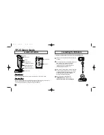
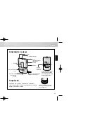
EXPLODED VIEWS

8-1. CASE SECTION

NOTE:

• Items marked “*” are not stocked since they are

seldom required for routine service. Some delay
should be anticipated when ordering these items.

• The mechanical parts with no reference number in

the exploded views are not supplied.

• Hardware (# mark) list and accessories and pack-

ing materials are given in the last of this parts list.

• Abbreviation

CND : Canadian model

The components identified by
mark 

!

 or dotted line with mark

!

 are critical for safety.

Replace only with part number
specified.

Les composants identifiés par une
marque 

!

 sont critiques pour la

sécurité.
Ne les remplacer que par une
piéce portant le numéro spécifié.

Ref. No.

Part No.

Description

Remark

Ref. No.

Part No.

Description

Remark

*

1

4-214-126-01 CASE

2

3-704-366-41 SCREW (CASE) (M3X6)

*

3

4-214-105-01 COVER (PS)

4

4-951-620-41 SCREW (2.6), +BVTP

*

5

4-224-380-01 PANEL, BACK

6

3-703-244-00 BUSHING (2104), CORD

*

7

1-672-165-11 LED BOARD

*

8

1-672-159-11 AC FILTER BOARD

*

9

1-672-162-11 D.SW BOARD

*

10

1-672-364-11 SCSI IN BOARD

*

11

1-672-365-11 SCSI OUT BOARD

*

12

1-672-161-11 P.JACK BOARD

*

13

1-672-166-11 DOUT BOARD

14

1-790-228-11 CORD (WITH CONNECTOR)

15

X-4948-515-1 ILLUMINATION ASSY

16

X-4946-543-2 FOOT (SMALL) ASSY

*

17

4-978-398-21 CUSHION

*

18

3-703-150-11 CLAMP

*

19

4-988-534-01 COVER, MOTOR

20

1-783-531-41 CORD, POWER

1

2

2

2

2

3

4

4

4

5

6

7

8

9

10

11

not supplied

not supplied

not supplied

not supplied

not supplied

not supplied

FRONT PANEL

12

13

14

15

16

17

17

#1

#2

#3

#3

#3

#3

#3

#3

#3

#3

#3

#9

#3

#3

#3

#3

#3

#3

#3

#3

#3

#3

18

19

20

Summary of Contents for CDJ-500

Page 1: ...MICROFILM CDJ 500 US Model Canadian Model SPECIFICATIONS SERVICE MANUAL CD ROM CHANGER Model Name Using Similar Mechanism NEW CD Mechanism Type CDM 56 Base Unit Type BU 24 Optical Pick up Type SPU3212 ...

Page 2: ...TIQUES POUR LA SÉCURITÉ DE FONCTIONNEMENT NE REMPLACER CES COMPOSANTS QUE PAR DES PIÈCES SONY DONT LES NUMÉROS SONT DONNÉS DANS CE MANUEL OU DANS LES SUPPLÉMENTS PUBLIÉS PAR SONY SAFETY CHECK OUT After correcting the original service problem perform the follow ing safety checks before releasing the set to the customer Check the antenna terminals metal trim metallized knobs screws and all other exp...

Page 3: ... 60 7 6 Schematic Diagram CD ROM Drive 2 6 Section 61 7 7 Schematic Diagram CD ROM Drive 3 6 Section 62 7 8 Schematic Diagram CD ROM Drive 4 6 Section 63 7 9 Schematic Diagram CD ROM Drive 5 6 Section 64 7 10 Schematic Diagram CD ROM Drive 6 6 Section 65 7 11 Schematic Diagram Main Section 66 7 12 Printed Wiring Board Main Section 67 7 13 Schematic Diagram Panel Section 68 7 14 Printed Wiring Boar...

Page 4: ...entially Operations are stopped when an error occurs Procedure 1 Set the DIP switches on the back panel as shown below 2 While pressing the OPEN button DISC SKIP button and DISC SKIP button simultaneously press the U button to turn ON the power When the CHANGER indicator starts to blink release the OPEN DISC SKIP and DISC SKIP buttons 3 The front door opens automatically 4 Close the front door to ...

Page 5: ...s ASPI manager Usable Version Aspi2dos sys 3 661J 3 68 3 68s Aspi4dos sys 3 34 3 35 3 36s 3 36s Aspi8dos sys 1 26 1 32 1 32s 1 32s General CD ROM SONY test disc TGRS 21 Green disc J 2501 110 A SCSI cable Speakers with amplifier or equivalent Use only when checking the AUDIO output Installing the FIELD50 EXE 1 Create the directory CDJC50S in the C drive of the PC used and copy the FIELD50 EXE file ...

Page 6: ...t SCSI TERM to ON and do not connect other SCSI equipment as much as possible 2 Set MODE to ON ON Normal mode Control the changer using the PC OFF Manual mode Control the changer manually using buttons 3 Setting of SCSI ID of the drive Set a desired ID number except 7 Be careful not to use an ID number already in use for the changer 4 Setting of SCSI ID of the changer Set a desired ID number excep...

Page 7: ...t the DOS prompt mode and execute the program 1 Turn on the power of the PC and set the DOS prompt mode 2 Change the directory to CDJC50S Enter a desired file name using less than 8 characters If numbers are used for the suffix of the file name these will be counted up automatically the next time When only the ENTER key is pressed the default file name will be set This file will be saved as the lo...

Page 8: ...d Enter 6 for the ID of the media changer to be checked using this program and press the ENTER key 7 The following screen appears Enter the serial number of the unit and press the ENTER key Enter the serial number of the unit 8 The number of the slot set with a disc will be displayed The screen asks whether the inspection is started Enter Y and press the ENTER key Displays the slot number s holdin...

Page 9: ...al number entered Enter A 10 The following screen appears and the front door opens auto matically Insert the general CD ROM into the 14th slot and close the door 11 The following screen appears and the front door opens auto matically Insert the SONY test disc TGRS 21 Green disc in the 1st slot and close the door Take note that if the door is closed without inserting any disc the following screen a...

Page 10: ...llowing appears at the bottom of the screen Check the audio signal here During this test analog audio signals are out put from the ANALOG OUT and digital audio signals from the DIGITAL OUT Check the sounds according to the instructions on the screen After completing preparations to check the sounds press the space key 14 When the following screen appears the 1 KHz sine wave is output from the L CH...

Page 11: ... file provided with the FIELD50 EXE software To end enter E or to continue enter the corresponding number 17 If there is a inspection to be executed again enter the corre sponding number and press the ENTER key To end enter E and press the ENTER key 18 The following screen appears at the bottom left of the screen Remove the disc and close the front door 19 The program is completed and the followin...

Page 12: ...oblems occurred the following will be displayed File name entered at step 5 SCSI bus device Structure of this unit detected on the SCSI bus Serial number entered at step 7 Slot number s holding a disc Test results ...

Page 13: ...s occurred the following is displayed inspection results Displayed when SCSI errors occur For details of the error codes displayed here refer to the PDF file of the instruction manual provided with the FIELD50 EXE program ...

Page 14: ...ID respectively CAUTION on SCREEN CHANGER LED FLASHING INSERT DISC MEDIA MAPPING OK START INSPECTION NO 1to6 General CD ROM disc into SLOT 14 Green disc into SLOT 1 Confirm the identification between real location and media mapping Select A on menu screen and start POWER LED lights green SCSI FAILURE HARDWARE ERROR KEY FAILURE DISC SENSOR FAILURE ...

Page 15: ...15 END NO 6 OK NO 2 OK NO 1 OK NO 3 to 5 OK START INSPECTION NO 1to6 SCSI INTEGRITY FAILURE AUDIO FAILURE GO DRIVE CHECK SECTION CHECK MECHANICAL PARTS ...

Page 16: ...3 Disc Sensor Error DISC SENSOR ADJUSTMENT DISC SENSOR S R MOUNT MAIN MOUNT HARNNES MAIN to DISC SENSOR S 4 Drive Chuck Error 04 53 83 MAIN MOUNT DRIVE UNIT FFC MAIN to MAC 30 5 Drive Unchuck Error 04 53 84 Equivalent to 4 6 Door Motor Error 04 53 85 D MOTOR MOUNT MAIN MOUNT HARNNES MAIN to D MOTOR KEY FAILURE KEY MOUNT HARNNES MAIN to KEY DISC SENSOR FAILURE DISC SENSOR ADJUSTMENT DISC SENSOR S R...

Page 17: ...an equivalent Setting the ASPI manager For details refer to Installing the ASPI manager on page 5 SCSI cable Connection SCSI LINE OUT DIGITAL OUT IN OUT SCSI TERM MODE ID SELECT 4 2 1 4 2 1 DRIVE CHANGER SCSI IN SCSI cable Accessory Connected to SCSI connector of the PC Fig Connection of equipment Setting DIP switch settings SCSI TERM MODE ID SELECT 4 2 1 4 2 1 DRIVE CHANGER 1 Set SCSI TERM to ON ...

Page 18: ...cribes the state where the DOS prompt is excuted from Windows 98 The following screen appears 3 Enter CD CDJC50S and press the ENTER key The follow ing screen appears 4 Enter UPDATEF and press the ENTER key The following screen appears If CDJ 500 is detected the number corresponded to SCSI adress is displayed Press the ENTER key to update program for this changer It is not necessary to enter numbe...

Page 19: ...le only press the ENTER key It is necessary enter number to downlord another HEX file 6 As the HEX file selected is displayed press the ENTER key Y is entered as the default 7 Revision 1 01 is rewritten to 1 02 and the display switches as follows The product information is still displayd old revision If downloaded successfully Finish Verifying is displayed If failed Failed Downloading or Failed Ve...

Page 20: ...iting failed If this unit does not operate normally after writing perform writ ing again using the following procedure 1 Remove the shield with the power OFF set the RECOVERY DIP switch to OFF press the U button and turn ON the power 2 Execute the UPDATEF and perform the writing process again using the method described earlier 3 After writing turn OFF the power of the unit once 4 Set the RECOVERY ...

Page 21: ...c AVA 2904E provided with this unit If not available use an equivalent ASPI manager setting For details refer to Installing ASPI manager on page 5 SCSI cable Connection SCSI LINE OUT DIGITAL OUT IN OUT SCSI TERM MODE ID SELECT 4 2 1 4 2 1 DRIVE CHANGER SCSI IN SCSI cable Accessory Connected to SCSI connector of the PC SCSI TERM MODE ID SELECT 4 2 1 4 2 1 DRIVE CHANGER 1 Set SCSI TERM to ON and do ...

Page 22: ...ect SYSTEM on the CONTROL PANEL on Windows 2 Display the CD ROM device from DEVICE MANAGER and select SONY CD ROM CDU625 See following diagram 3 Uncheck Sync data transfer and Auto insert notification at this screen 4 Restart and the changes made will be set Uncheck Sync data transfer Uncheck Auto insert notification ...

Page 23: ...n Windows 95 98 The following describes the state where the DOS prompt is ex ecuted from Windows 98 The following screen appears 3 Set the directory copied with the program at item 1 Enter CD CDJC50S and press the ENTER key 4 Enter DWN ASPI and press the ENTER key The following screen appears The following explains the example of rewriting the program 1 0W of the drive with 1 0Y The HEX file in th...

Page 24: ... name checked at step 6 as DWN ASPI 625_XXX and press the ENTER key File name copied at item 1 8 The following screen appears Check that the HEX file is cor rect and enter Y 9 The following screen appears If the ID is correct enter Y When N is entered the CD ROM drive of another ID will be detected The version of the program currently set ...

Page 25: ...25 10 The following screen appears Press the ENTER key 11 The following screen appears and files are downloaded one by one ...

Page 26: ...26 Newly rewritten program version 12 When downloading is finished the following screen appears ...

Page 27: ... through the CD ROM device name changes to CD ROM LOADER Check system environment espe cially SCSI configration To download another time select this device The screen shows the following for step 10 14 To end press the ESC key 15 The POWER indicator and CHANGER indicator of the unit light up To set the changes press the U button to turn OFF the power and press it again to turn ON the power again ...

Page 28: ...2 Grounding for the work table Be sure to lay a conductive sheet with impedance lower than 109 Ω on the table such as a sheet of copper which is ground 3 As static electricity built up on clothes does not drain away be careful not to let your clothes touch the unit Flexible cable 1MΩ 2Conductive sheet or copper plate 1Wrist Strap for grounding 1MΩ Base unit assy 4 Do not apply excessive force to t...

Page 29: ...N OF PARTS AND CONTROLS Front Panel 1 u button 2 Emergency eject hole 3 OPEN button 4 POWER indicator 5 DRIVE indicator 6 CHANGER indicator 7 DISC SKIP button 8 DISC SKIP button SECTION 2 GENERAL 2 3 4 7 5 6 1 8 ...

Page 30: ...To MAIN board Two screws BVTT3x6 Beam Flat type wire 9 core Bracket illumination with illumination assy MAIN borad CN602 MAIN borad CN601 Claw Expand the front panel in the direction of arrow to release catching claws Claw Expand the front panel in the direction of arrow to release catching claws 9 0 Six screws BVTT3x10 Front panel Screw BVTT3x6 Two screws BVTT3x6 Two clamps Connector ...

Page 31: ...NISM DECK 1 2 3 4 5 6 7 8 9 0 ª Screw PTPWH2 6x8 Table 50 Ring B2 Two screws BV SUMITITE B3 Connector DISC SENSOR S board CN53 CD mechanism deck Flat type wire 12 core Connector TABLE SENSOR board CN51 Connector TABLE SENSOR board CN52 Connector MOTOR board CN61 Connectotr Connectotr Connectotr Earth wire Three screws BVTT3x10 Screw BVTT3x14 Screw BVTT3x10 Connector SW board CN54 CD mechanism base...

Page 32: ...crews BTP2 6x8 Two screws PTPWH2 6x8 Screw PTPWH2 6x8 Screw P 2x4 PC board assy BU holder assy Magnet holder Torsion spring Holder Two screws M step Two screws M step Base unit Leaf spring BU 5 9 0 Remove the torsion spring and take out the magnet holder with pulling up the claw toward you ...

Page 33: ... in the figure when attaching 4 5 6 7 8 1 2 3 9 Screw BTP2 6x8 Screw BTP2 6x8 Screw BTP2 6x8 Screw PTPWH M2 SW board Cam cover Slider Loading Torsion spring Loading Disc holder A2 Loading lever Assy Tension coil spring Lever Cover Lever Disc holder B Slider Lock Slider Cam 0 ...

Page 34: ...s the U button to turn OFF the power 6 While pressing the OPEN button DISC SKIP button and DISC SKIP button simultaneously press the U button to turn ON the power Keep on pressing three buttons untill CHANGER LED is flasing 7 Continue pressing the DISC SKIP button until loading end 8 Rotate the pulley with finger Fig 2 to stop the disc holder A2 slightly away from the disc Fig 3 9 Check that disc ...

Page 35: ...tton until loading in again 12 Check that the disc is at the position adjusted to in step 7 13 Continue pressing the DISC SKIP button until loading end 14 Visually check the chucking pulley and adjust the adjusting screw B shown in the figure so that the positional relation of the holder magnet and chucking pulley satisfies the specified val ues Fig 4 Fig 5 A B Holder Chucking pulley No clearance ...

Page 36: ...clockwise direction 5 Loosen the fixed screw C to move the holder sensor R and secure it when the H portion of the T P waveform of the oscillo scope comes to the center of the H portion of the SENSOR wave form 6 Press the DISC SKIP button The disc table starts to rotate in the counterclockwise direction 7 Check that the waveform on the oscilloscope is the same as that adjusted in step 5 Repeat fro...

Page 37: ...ools IBM PS VP System PS VP and the monitor 640kbyte RAM 3 5 FDD HDD Video RAM CGA or Higher DOS Ver 6 2 or later SCSI boardAVA 2904E that is supplied as an accessory of CDJ 500 or equivalent Active Speaker SCSI cable Attached or equal cable 5 1 1 3 Test Disc SONY Test Disc YEDS 18 3 702 101 01 SONY Test Disc TGRS 21 J 2501 110 A 5 1 1 4 Measuring Equipments Osilloscope Dual Trace 20MHz probe x10 ...

Page 38: ... DIP SW 1 to 4 are OFF AHA 2940 for PCI BUS AVA 2904E for PCI BUS No Jumper and SW setting on the board Use default parameter for SSI Select configuration utility It is not necessary to install the device driver when using on the windows 95 It is necessary to install the device driver at first line of config sys when using on DOS c Install the SCSI Interface board in the PS VP System PS VP System ...

Page 39: ...39 Function check ON OFF SCSI TERM MODE SCSI TERM ON MODE OFF ID2 ID1 ID0 PARITY S706 S707 TEST SW601 CDM 56 Dip SW Dip SW MAIN PCB MAIN BOARD Note It is not needed to disconnect the internal SCSI cable ...

Page 40: ... or not a Poor connection with the host system esp GND related connection frame GND etc b Incorrect operational procedure 5 2 2 FLOWCHART FOR TROUBLE SHOOTING c Program error of host system d The SCSI TERM of DIP SW on the rear of set is not set to ON e Wrong Drive Number selection f Wrong supply voltage g Environmental conditions where electrical noise easily jumps into signal h Influence of stro...

Page 41: ...udio X Talk L R 18 Play Audio X Talk R L 19 Sub Code Read 5 2 3 PROCEDURE OF ATP TEST 5 2 3 1 Pre setting a Connect the CDJ 500 to the Computer Refer to Fig 5 1 3 2 b Set the Jumpers on theAdaptec SCSI board Refer to Fig 5 1 3 2 c Set the COMMAND SW of back panel as below Hit any key to start or Esc to exit Drive Status Column Display 5 2 3 1 a ID2 OFF ID1 ON ID0 ON PARITY ON d Turn on the power o...

Page 42: ...m 1 3 seek test quadruple will be executed n Full seek test Max will be executed o 1 3 seek test Max will be executed 2 After Seek test completion Play Audio DeTRCK test will be executed a Hit any key when ready message will be displayed on the drive status column then hit any key b Play Audio E Volume test will be executed c Any key when Okay or Esc when NG message will be dis played on the drive...

Page 43: ...any key when ready OK Sony SCSI CD ROM Failure Verification Test Ver 1 00 00 Nov 22 1996 ID 7 ASW 1210 V 3 60 ADAPTEC AHA 1520ADAPTEC AHA 1520 ATP625 CFG 0 Inquiry check Pass ID 3 SONY CD ROM CDU625 X Xx 1 TEST UNIT READY Pass READY 2 TOC read Pass 3 Incremental Read Pass 4 Random Seek Read Pass 5 Spin Up Down X1 Pass Spin Up XXXX ms Spin Down XXX ms 6 Spin Up Down X4 Pass Spin Up XXXX ms Spin Dow...

Page 44: ...f CD DSP IC The page 23 shows the sequence of execution items in Power On ResetActions It will help you finding any defective point on the drive to know the specified processing sequence of the auto adjustment items and drive s action in the Power On Re set Actions Preparing The following tools and measuring equipments are necessary for performing this section Oscilloscope Sony Test Disc YEDS 18 3...

Page 45: ...led NG NG Access Time NG Read Data Error IC301 CDROM SCSI I F IC failure IC302 buffer RAM failure IC201 CD DSP servo IC failure Motor Driver ICs failure IC301 CDROM SCSI I F IC failure IC304 Flash ROM failure Refer to Flowchart 2 Power on Reset Actions IC201 CD DSP servo IC failure IC101 RF Amp IC failure Drive ICs failure BU OP checking Replace BU HP PWB checking IC303 CPU failure IC305 gate arra...

Page 46: ...ed in Step 16 21 Read TOC Set x8 speed OK Completed Try Read operation IC101 IC201 IC106 IC101 IC201 IC101 IC106 Focus Search Refer to 5 2 4 6 Spindle Motor Driver IC Refer to 5 2 4 11 RF Signal Refer to 4 2 4 13 Check Focus Tracking Servo Error Signal RF Signal Refer to 5 2 4 13 RF Signal Refer to 5 2 4 13 Spindle Motor Driver IC Refer to 5 2 4 11 NG NG NG Retry for detailed checking OK Passed OK...

Page 47: ...Track Servo Gain Auto Adjustment sync pattern detection Disc Diameter 8cm 12cm Detection Read TOC Jump to 00 02 00 Subcode Q detection Disc Linear Speed Detection Set max rotational speed sync pattern detect subcode Q detection Completed Drive Action LD to turn on OP lens to move up and down You will hear a small beep sound from the drive during these auto adjustment You will see RF Signal with Sp...

Page 48: ...ty is not good check servo circuit 5 2 4 8 Laser Power Check Laser beam a Disassemble the drive so that the optical device is exposed b Turn on the drive power and look into the objective lens care fully while the drive is in process of focus search c Check if the red beam comes out from the optical pick up Warning Do not look into LD beam closely with naked eyes d In case of no beam from optical ...

Page 49: ...Listen the sound from the drive while the drive is spinning up b Check if there is any slipping noise among the Turntable the Chucking Pulley Ass y and the Disc c If you hear any check the mechanical adjustments SECTION 4 d Otherwise disassemble the drive and check if there is excessive dust or any contamination on the Turntable or the disc Note As the CD 56 adopts the VCAN Vibration Cancel motor ...

Page 50: ...rm the following A B x 100 less than 22 ID2 ON ID1 ON ID0 ON PARITY OFF 5 2 4 12 RF Level Note Before performing electrical block checks solder a lead wire to TP RFEQ and TP VC of the MA C30 board Chuck the disk YEDS 18 beforehand Refer to 5 2 4 1 and set the test mode Press the OPEN button to open the door place the disc in the slot in front close the door to chuck the disc 1 Connect the oscillos...

Page 51: ...tion MA C30 BOARD Side B ON OFF SCSI TERM MODE ID2 ID1 ID0 PARITY S706 S707 TEST SW601 TP RF RF EQ RF Level Check CNJ201 CNJ104 CNJ103 CNJ102 IC106 IC104 IC110 TP VC RF Level Check EF balance Check TP TE EF balance Check ...

Page 52: ...is not issued to the drive for more than the inactivity time which can be set by mode select command the drive goes into standby mode automatically Any command that requires disc access can resume the drive from standby mode SECTION 6 THEORY OF OPERATION P CAV Drive By using latest P CAV partical CAV technology the CDM 56 re alizes data transferring with variable transfer rate from 12 in ner track...

Page 53: ... board SCSI IN board SCSI OUT board P SW board P JACK board DOOR MOTOR board POWER board D SW board AC FILTER board KEY board D OUT board MOTOR board CHUCK SW board TABLE SENSOR board DISC SENSOR S board DISC SENSOR R board MA C30 board SE C7 board ...

Page 54: ...IO 1 59 IO 0 2VRO 69 70 X201 40MHz PXI PXO DIGITAL SERVO DIGITAL SIGNAL PROCESSOR IC201 RF3 SHOCK SENSOR SLED MOTOR SPEED SENSOR M M002 SLED MOTOR 85 BUS 0 86 BUS 1 87 BUS 2 88 BUS 3 91 BUCK 92 XCCE 95 XRST 12 9 26 8 DV BYPS DV 14 15 19 11 25 13 7 CB CB VL CTRL VLO DVO 32 18 27 17 31 28 16 SRDR SFDR SLCON TKC A B CA A B CA 22 29 25 26 23 24 27 100 3 7 2 6 4 DOUT LRCK BCK C2P0 SBS SBCK VCOREF PDOS ...

Page 55: ...1 VSG SLCON 79 SLCON 77 SLCON 74 TKC 66 SLDOP 65 SLDOM 62 HVDET B 61 HVDET A 13 15 17 21 12 5 27 26 23 25 4 28 29 3 28 29 13 14 80 PARITY 7 PWEN 22 24 31 SCSI CONTROL BUS SLDOM SLDOP TKC SLCON SLCON SIGNAL PATH DATA MDT LRCK BCK C2P0 SBS SFSY SBSY SBDK SBCK XAMUTE DCLK XRESET BUS 0 BUS 1 BUS 2 BUS 3 XCCE BUCK VSG RF 1 FLG A FLG B FLG C FLG D LOCK GVSW TRBST DRVEN HVDET A HVDET B BCK SBCK SFSY SBS ...

Page 56: ...CE 22 OE 27 WE IC605 ADDRESS DECODER M M M VCC BUFFER Q601 12V M61 LOADING MOTOR M62 TABLE MOTOR M005 DOOR MOTOR S706 707 XO KEY XL KEY XR KEY S703 705 KEY SW OPEN REW RF DISC SENSOR TABLE SENSOR1 3 IC51 53 T SENS1 3 Q51 D SENS DB0 DB7 DBP ATN BSY ACK RST MSG SEL C D REQ I O X602 40MHz RESET IC608 5V TIN TOUT XEJECT CHUCK U CHK D ID0 D ID1 D ID2 C TIN TOUT XEJECT CHUCK U CHK D ID0 D ID1 D ID2 D SE...

Page 57: ...led numbers refer to waveforms Signal path J CD F AUDIO Abbreviation CND Canadian model 1 2 3 4 WAVEFORMS CD ROM SECTION PLAY IC101 RFGO Indication of transistor C These are omitted E B Caution Pattern face side Parts on the pattern face side seen from the Side B pattern face are indicated Parts face side Parts on the parts face side seen from the Side A parts face are indicated Q C These are omit...

Page 58: ...D CD ROM DRIVE SECTION See page 53 for Circuit Boards Location Semiconductor Location Ref No Location IC104 B 4 IC106 B 5 IC110 B 5 IC112 B 2 IC501 B 2 Q205 C 2 Q206 C 2 Q701 A 2 Page 69 Page 67 Page 75 Page 71 Page 69 TP VC TP TE TP RFEQ ...

Page 59: ...onductor Location Ref No Location D101 B 1 D201 C 3 D301 D 1 D701 B 5 IC101 A 2 IC103 A 3 IC105 B 3 IC107 A 3 IC109 B 1 IC111 B 4 IC201 C 4 IC202 B 3 IC203 C 3 IC301 D 4 IC302 D 3 IC303 D 3 IC304 D 1 IC305 D 1 Q101 A 1 Q102 B 2 Q103 A 2 Q104 B 2 Q105 B 2 Q106 C 2 Q202 B 4 Q203 C 3 Q207 B 3 Q702 A 4 Page 67 ...

Page 60: ...CDJ 500 60 60 7 5 SCHEMATIC DIAGRAM CD ROM DRIVE 1 6 SECTION See page 57 for Waveforms See page 76 for IC Block Diagrams Page 70 Page 62 Page 62 Page 61 Page 68 Page 68 Page 63 Page 64 ...

Page 61: ...CDJ 500 61 61 7 6 SCHEMATIC DIAGRAM CD ROM DRIVE 2 6 SECTION See page 57 for Waveforms See page 76 for IC Block Diagrams Page 62 Page 62 Page 62 Page 60 ...

Page 62: ...62 7 7 SCHEMATIC DIAGRAM CD ROM DRIVE 3 6 SECTION See page 57 for Waveforms See page 76 for IC Block Diagrams Page 60 Page 61 Page 61 Page 61 Page 64 Page 64 Page 64 Page 64 Page 64 Page 64 Page 64 Page 66 Page 60 ...

Page 63: ...63 63 7 8 SCHEMATIC DIAGRAM CD ROM DRIVE 4 6 SECTION See page 57 for Waveforms See page 78 for IC Block Diagrams See page 83 for IC Pin Functions Page 60 Page 64 Page 64 Page 64 Page 65 Page 65 Page 74 Page 66 ...

Page 64: ...DIAGRAM CD ROM DRIVE 5 6 SECTION See page 57 for Waveforms See page 78 for IC Block Diagrams See page 86 for IC Pin Functions Page 60 Page 62 Page 62 Page 62 Page 62 Page 62 Page 62 Page 62 Page 63 Page 63 Page 63 Page 65 Page 65 ...

Page 65: ...CDJ 500 65 65 7 10 SCHEMATIC DIAGRAM CD ROM DRIVE 6 6 SECTION See page 57 for Waveforms See page 79 for IC Block Diagrams Page 63 Page 63 Page 64 Page 64 ...

Page 66: ... 7 11 SCHEMATIC DIAGRAM MAIN SECTION See page 80 for IC Block Diagrams See page 88 for IC Pin Functions Page 68 Page 68 Page 62 Page 70 Page 68 Page 68 Page 68 Page 68 Page 74 Page 68 Page 74 Page 63 Page 72 Page 72 ...

Page 67: ...miconductor Location Ref No Location IC601 D 4 IC602 C 3 IC604 C 2 IC605 B 2 IC606 B 2 IC607 D 1 IC608 D 1 IC609 B 3 IC610 B 1 Q601 D 3 Semiconductor Location Ref No Location IC603 C 2 Page 69 Page 69 Page 69 Page 59 Page 69 Page 69 Page 69 Page 69 Page 75 Page 71 Page 73 Page 73 Page 58 Page 75 ...

Page 68: ...CDJ 500 68 68 7 13 SCHEMATIC DIAGRAM PANEL SECTION Page 60 Page 60 Page 66 Page 66 Page 66 Page 66 Page 72 Page 66 Page 66 Page 66 ...

Page 69: ...CDJ 500 69 69 7 14 PRINTED WIRING BOARD PANEL SECTION See page 53 for Circuit Boards Location Page 58 Page 67 Page 67 Page 67 Page 67 Page 67 Page 58 Page 67 Page 73 Page 67 ...

Page 70: ...CDJ 500 70 70 7 15 SCHEMATIC DIAGRAM SENSOR SECTION Page 60 Page 66 ...

Page 71: ...CDJ 500 71 71 7 16 PRINTED WIRING BOARD SENSOR SECTION See page 53 for Circuit Boards Location Page 71 Page 67 ...

Page 72: ...CDJ 500 72 72 7 17 SCHEMATIC DIAGRAM SCSI SECTION Page 68 Page 74 Page 66 Page 66 ...

Page 73: ...CDJ 500 73 73 7 18 PRINTED WIRING BOARD SCSI SECTION See page 53 for Circuit Boards Location Page 73 Page 69 Page 67 Page 75 ...

Page 74: ...CDJ 500 74 74 7 19 SCHEMATIC DIAGRAM POWER SECTION See page 82 for IC Block Diagrams Page 66 Page 66 Page 72 Page 63 ...

Page 75: ...ARD POWER SECTION See page 53 for Circuit Boards Location Semiconductor Location Ref No Location D902 D 2 D903 B 2 D904 B 3 D905 C 1 D906 C 1 D907 C 1 D908 C 1 IC901 C 2 IC902 C 3 IC903 B 1 Ref No Location Page 67 Page 58 Page 67 Page 73 ...

Page 76: ...HUT DOWN BUFFER AMP1 BUFFER AMP2 RF RF GND VIN1 VIN1A MUTE1 VIN2 VIN2A VIN3 VIN3A BUFFER OUT1 BUFFER OUT2 VCC RF RF RF RF VS1 VREF1 UOUT UOUT VOUT VOUT WOUT WOUT VS2 MUTE2 N C RF RF IC105 TC4W53FU IC106 BA6849FP E2 IC107 LA6527N 8 7 6 5 1 2 3 4 VCC CH1 CH0 ADR COM INH VEE VSS 9 22 23 24 28 27 26 25 20 18 17 15 4 2 7 8 10 11 12 13 14 D R TORQUE SENSE AMP Q CK Q 21 GAIN CONTROL DRIVER TSD TL PS A3 A...

Page 77: ... 73 72 71 70 69 68 67 66 65 64 63 62 61 60 59 58 57 56 55 54 53 52 51 50 49 48 47 46 45 44 43 42 41 40 39 38 37 36 35 34 33 32 31 30 29 28 27 26 LPF 1 BIT DAC MICRO COMPUTER INTERFACE CLOCK GENERATOR ADDRESS CIRCUIT ERROR CORRECTOR PWM ROM RAM D A PWM VCO PLL TMAX DATA SLICER SYNC SIGNAL PROTECT EFM DEMODULATOR STATUS CLV SERVO SERVO CONTROL DIGITAL EQUALIZER AUTOMATIC ALIGNMENT CIRCUIT 16K RAM DI...

Page 78: ...SS V SS V DD V DD V DD V DD V DD V DD XDB0 XDB1 XDB3 XDB4 XDB5 XDB6 XDB7 XDBP XATN XBSY XACK XRST XWSG XSEL XDB2 V SS V SS V SS V SS V SS V SS V SS V SS V SS V SS V SS V SS V SS V SS VDD XWAT A0 A1 A2 A3 A4 A5 A6 D0 D2 D1 D3 D4 D5 D6 D7 INT XCS XWR XRD DESCRAMBLER PRIORITY RESOIVER DMA SEQUENCER SYNC CONTROL FIFO CONTROL 24BIT TRANSFER BYTE COUNTER BUFFER HANDSAKE SCSI HANDSAKE SCSI PHASE CTRL ARB...

Page 79: ... 1 TIOCA 4 TP 10 PB 2 TIOCB 4 TP 11 PB 3 TOCXA 4 TP 12 PB 4 TOCXB 4 TP 13 PB 5 TP 14 PB 6 TXD P9 0 D 0 P3 0 D 1 P3 1 D 2 P3 2 D 3 P3 3 D 4 P3 4 D 5 P3 5 D 6 P3 6 D 7 P3 7 A17 P52 A16 P51 A15 P27 A14 P26 A13 P25 A12 P24 A11 P23 A9 P21 A10 P22 A8 P20 A7 P17 A6 P16 A5 P15 A4 P14 A3 P13 A2 P12 A1 P11 A0 P10 VCC VSS P7 1 AN 1 P7 0 AN 0 P6 5 WR P6 4 RD P6 3 AS VCC EXTAL VSS NMI RES STBY Ø XTAL MD 1 MD 0...

Page 80: ...UT RIN1 IOUT VEE VEE VCC VREF VREG VCC OUT1 OUT1 18 17 16 15 1 2 3 4 5 6 7 8 9 14 13 12 11 10 IC605 SN74HC138ANS IC608 M51953BFP 1 2 3 4 5 6 7 8 9 10 11 12 13 14 15 16 17 18 19 20 Q OE D0 D1 D2 D3 D4 D5 D6 D7 GND OE D VCC Q0 Q1 Q2 Q3 Q4 Q5 Q6 Q7 LE G Q OE D G Q OE D G Q OE D G Q OE D G Q OE D G Q OE D G Q OE D G 15 14 13 12 11 10 9 8 7 6 5 4 3 2 1 GND Y7 G1 G2B G2A C B A A B C G2A Y7 G1 G2B Y6 Y5 ...

Page 81: ... CONVERTER REALTIME OUTPIT PORT BUS VF TIMER COUNTER 0 16 BIT PORT 7 VSS RESET X1 VDD X2 TEST VSS ASTB CLKOUT P40 A00 P41 A01 P42 A02 P12 ASCK2 SCK2 P11 PWM1 P10 PWM0 P15 P14 Tx02 S02 P17 P16 P13 Rx02 S12 P72 AN12 P71 AN11 P74 AN14 P73 AN13 P70 AN10 VDD P35 T01 P36 T02 P37 T03 P32 SCL P33 SDO SDA P34 T00 P03 P04 P05 P06 P07 P67 REFRQ HLDAK P00 P01 P02 P44 A04 P43 A03 P47 A07 P46 A06 P45 A05 P54 A1...

Page 82: ...4166D2TR4 1 5 VOLTAGE FEEDBACK INPUT SWITCH OUTPUT GND INPUT VOLTAGE VCC COMPEN SATION 2 THERMAL SHUTDOWN 5 05V REFERENCE OSCILLATOR ERROR AMP B B S R Q B UNDER VOLTAGE LOCKOUT PULSE WIDTH MODULATOR CURRENT SENSE PWM LATCH 3 4 ...

Page 83: ...pply 5V SCSI data bua bit2 Ground SCSI data bus bit3 SCSI data bus bit4 Ground Ground Power supply 5V SCSI data bus bit5 Ground SCSI data bus bit6 Ground SCSI data bus bit7 Ground Power supply 5V SCSI data bus parity Ground SCSI control bus ATN signal Ground SCSI control bus BSY signal Ground Power supply 5V SCSI control bus ACK signal SCSI control bus RST signal Ground Ground Power supply 5V Grou...

Page 84: ...o buffer memory Buffer memory RAS Row Address Strobe signal Buffer memory CAS Column Address Strobe signal Buffer memory CAS Column Address Strobe signal Buffer memory data write strobe signal Ground Power supply 5V Buffer memory data bus bit0 Buffer memory data bus bit1 Buffer memory data bus bit2 Buffer memory data bus bit3 Buffer memory data bus bit4 Buffer memory data bus bit5 Buffer memory da...

Page 85: ...ut to DAC Connected to CXD3000 LRCKI pin pin 26 Output for GRSCOR resyncronizing Connected to CXD3000 SCSY pin pin 68 DSP RAM Overflow input Connected to CXD3000 ROF pin pin 45 Test pin0 Test pin1 Test pin2 Test pin3 Ground Test pin4 Test pin5 Test pin6 Test pin7 Ground Power supply 5V Wait signal for sub CPU buffer memory access CXD1804R built in register address bus0 CXD1804R built in register a...

Page 86: ...I O I O I O I O I O I O I O I O I O I O I O I O I I I I I I I I O I I I O I I I I I Switch Switch Ground Ground Switch Headphone mute Audio mute LED LED Ground Power supply DSP reset CPU Monet reset Reset Reset Not used DSP subcode sync DSP DSP DSP DSP DSP DSP Ground CPU data bus CPU data bus CPU data bus CPU data bus CPU data bus CPU data bus CPU data bus CPU data bus CPU address bus CPU address ...

Page 87: ...AV0 CAV VDD EXC0 EXC1 GND TEST PWM1 DCK CCK PWM0 O O O O O O I I O O O O Spindle driver 1 on Spindle driver 0 on CLV on CAV on Spindle control Power supply 33 86MHz 16 93MHz Ground Ground Control the outside spindle motor DSP clock 33 86MHz DSP clock 33 86MHz Control the outside spindle motor ...

Page 88: ...ontroller DMA write signal 5V Power supply DMA data bus DMA data bus DMA data bus Ground DMA data bus DMA data bus DMA data bus Ground DMA data bus DMA data bus Odd parity for DB7 0 Power supply SCSI data signal SCSI data signal SCSI data signal Ground SCSI data signal SCSI data signal SCSI data signal SCSI data signal Ground SCSI data signal SCSI data signal Schmitt trigger input SCSI output Grou...

Page 89: ...VSS PAD4 PAD5 PAD6 PAD7 VDD I I I O I O I O I O I O I O I O I O Ground Address inputs Address inputs Ground Processor address data Processor address data Processor address data Processor address data Ground Processor address data Processor address data Processor address data Processor address data Power supply ...

Page 90: ... numéro spécifié Ref No Part No Description Remark Ref No Part No Description Remark 1 4 214 126 01 CASE 2 3 704 366 41 SCREW CASE M3X6 3 4 214 105 01 COVER PS 4 4 951 620 41 SCREW 2 6 BVTP 5 4 224 380 01 PANEL BACK 6 3 703 244 00 BUSHING 2104 CORD 7 1 672 165 11 LED BOARD 8 1 672 159 11 AC FILTER BOARD 9 1 672 162 11 D SW BOARD 10 1 672 364 11 SCSI IN BOARD 11 1 672 365 11 SCSI OUT BOARD 12 1 672...
Page 91: ...NG TORSION 60 4 212 600 01 GEAR CAM 61 4 212 612 01 GEAR A 62 X 4950 368 1 BRACKET DL ASSY 63 3 354 963 32 DAMPER 64 A 4724 449 A KEY A BOARD COMPLETE 65 4 217 468 01 SCREW 2 6X8 66 1 672 164 11 DOOR M BOARD 67 4 212 818 01 CUSHION W 68 4 212 819 01 CUSHION B 69 4 217 302 01 CUSHION B2 70 X 4951 511 1 DOOR MOTOR ASSY M901 1 541 590 11 MOTOR DC 5 M901 not supplied not supplied not supplied not supp...

Page 92: ...YPE 12 CORE 112 1 790 231 11 WIRE FLAT TYPE 12 CORE 113 A 4724 461 A MAIN BOARD COMPLETE T901 1 433 542 11 TRANSFORMER POWER 114 3 970 608 41 BV SUMITITE B3 Les composants identifiés par une marque sont critiques pour la sécurité Ne les remplacer que par une piéce portant le numéro spécifié The components identified by mark or dotted line with mark are critical for safety Replace only with part nu...

Page 93: ...SSY CHUCKING 220 4 214 316 01 COVER PULLEY 221 3 910 095 11 RUBBER VIBRATION PROOF 222 X 4950 566 1 BRACKET DS ASSY 223 1 672 170 11 DISC SENSOR S BOARD 224 4 214 267 01 BALANCER K2 225 4 214 268 01 BALANCER K3 226 4 214 269 01 BALANCER K4 227 4 974 711 01 SCREW 2X5 P TYIGHT PTTWH 228 4 981 923 01 SCREW M STEP 229 X 4950 567 1 HOLDER ASSY BU 230 7 624 101 04 STOP RING 1 2 E TYPE 231 4 214 137 01 R...

Page 94: ...8 425 01 PULLEY 255 4 988 424 01 GEAR TABLE 256 4 988 423 01 GEAR A LOADING 257 4 988 432 01 GEAR B LOADING 258 1 672 169 11 DISC SENSOR R BOARD 259 8 729 926 31 PHOTO TRANSISTOR PT483F1 260 4 990 669 01 HOLDER SENSOR 261 4 988 426 01 BASE CDM 262 1 672 167 11 MOTOR BOARD M61 X 4591 512 1 MOTOR ASSY LOADING M62 X 4591 512 1 MOTOR ASSY TABLE 251 252 252 252 253 254 254 255 256 258 257 259 260 261 2...

Page 95: ...313 4 974 767 01 SPRING COMPRESSION 314 4 973 786 01 GEAR S C1 315 A 4683 012 A GEAR ASSY B LIMITTER 317 4 993 513 03 INSULATOR K 318 4 974 725 01 SCREW M1 7X2 5 P 303 1 790 251 11 WIRE FLAT TYPE 11 CORE M101 A 4672 641 A SPINDLE ASSY SPINDLE M102 X 4951 510 1 MOTOR DC SLED Les composants identifiés par une marque sont critiques pour la sécurité Ne les remplacer que par une piéce portant le numéro...

Page 96: ...N902 1 580 230 11 PIN CONNECTOR PC BOARD 2P CN903 1 564 321 00 PIN CONNECTOR 2P CN904 1 568 226 11 PIN CONNECTOR 2P COMPOSITION CIRCUIT BLOCK CP902 1 537 771 21 TERMINAL BOARD GROUND FUSE F901 1 532 388 51 FUSE 2A 250V FUSE HOLDER FH901 1 533 293 11 FUSE HOLDER FH902 1 533 293 11 FUSE HOLDER TRANSFORMER T902 1 416 321 11 COIL LINE FILTER T901 1 433 542 11 TRANSFORMER POWER 1 672 171 11 CHUCK SW BO...

Page 97: ...TOR 2P DIODE D841 8 719 058 17 DIODE LNG401NPYJA D842 8 719 058 17 DIODE LNG401NPYJA D843 8 719 058 17 DIODE LNG401NPYJA RESISTOR R841 1 216 029 00 METAL CHIP 150 5 1 10W R842 1 216 029 00 METAL CHIP 150 5 1 10W R843 1 216 029 00 METAL CHIP 150 5 1 10W A 4724 437 A MA C30 BOARD COMPLETE CAPACITOR C101 1 164 004 11 CERAMIC CHIP 0 1uF 10 25V C102 1 164 004 11 CERAMIC CHIP 0 1uF 10 25V C103 1 124 778...

Page 98: ... 1 164 004 11 CERAMIC CHIP 0 1uF 10 25V C224 1 164 004 11 CERAMIC CHIP 0 1uF 10 25V C227 1 164 004 11 CERAMIC CHIP 0 1uF 10 25V C228 1 164 004 11 CERAMIC CHIP 0 1uF 10 25V C229 1 164 004 11 CERAMIC CHIP 0 1uF 10 25V C230 1 164 004 11 CERAMIC CHIP 0 1uF 10 25V C233 1 115 363 11 CERAMIC CHIP 10uF 10V C234 1 115 363 11 CERAMIC CHIP 10uF 10V C235 1 163 251 11 CERAMIC CHIP 100PF 5 50V C236 1 163 251 11...

Page 99: ...10 5 1 10W R113 1 216 001 00 METAL CHIP 10 5 1 10W R114 1 216 001 00 METAL CHIP 10 5 1 10W R115 1 216 001 00 METAL CHIP 10 5 1 10W R118 1 216 295 91 SHORT 0 R119 1 216 673 11 METAL CHIP 8 2K 0 5 1 10W R120 1 216 295 91 SHORT 0 R121 1 216 673 11 METAL CHIP 8 2K 0 5 1 10W R122 1 216 001 00 METAL CHIP 10 5 1 10W R123 1 216 663 11 METAL CHIP 3 3K 0 5 1 10W R124 1 216 651 11 METAL CHIP 1K 0 5 1 10W R12...

Page 100: ... CHIP 22K 0 5 1 10W R247 1 216 121 91 RES CHIP 1M 5 1 10W R249 1 216 667 11 METAL CHIP 4 7K 0 5 1 10W R250 1 216 663 11 METAL CHIP 3 3K 0 5 1 10W R251 1 216 655 11 METAL CHIP 1 5K 0 5 1 10W R256 1 216 097 91 RES CHIP 100K 5 1 10W R257 1 216 097 91 RES CHIP 100K 5 1 10W R308 1 216 001 00 METAL CHIP 10 5 1 10W R310 1 216 073 00 METAL CHIP 10K 5 1 10W R311 1 216 033 00 METAL CHIP 220 5 1 10W R316 1 2...

Page 101: ...SISTOR R601 1 216 041 00 METAL CHIP 470 5 1 10W R602 1 216 041 00 METAL CHIP 470 5 1 10W R603 1 216 073 00 METAL CHIP 10K 5 1 10W R604 1 216 085 00 METAL CHIP 33K 5 1 10W R605 1 216 073 00 METAL CHIP 10K 5 1 10W R606 1 216 073 00 METAL CHIP 10K 5 1 10W R607 1 216 073 00 METAL CHIP 10K 5 1 10W R608 1 216 073 00 METAL CHIP 10K 5 1 10W R609 1 216 073 00 METAL CHIP 10K 5 1 10W R610 1 216 073 00 METAL ...

Page 102: ...CTOR 4P CN907 1 691 766 21 PLUG MICRO CONNECTOR 4P CN908 1 568 951 11 PIN CONNECTOR 2P CN909 1 568 951 11 PIN CONNECTOR 2P COMPOSITION CIRCUIT BLOCK CP901 1 537 771 21 TERMINAL BOARD GROUND DIODE D902 8 719 025 03 DIODE RBA 402 SL D903 8 719 210 39 DIODE EC10QS 04 D904 8 719 210 39 DIODE EC10QS 04 D905 8 719 210 33 DIODE EC10DS2 D906 8 719 210 33 DIODE EC10DS2 D907 8 719 210 33 DIODE EC10DS2 D908 ...

Page 103: ...OR IC IC691 8 759 464 52 IC BH9598FP YE2 RESISTOR R691 1 216 073 00 METAL CHIP 10K 5 1 10W 1 672 168 11 TABLE SENSOR BOARD CONNECTOR CN51 1 568 944 11 PIN CONNECTOR 6P CN52 1 506 481 11 PIN CONNECTOR 2P IC IC51 8 749 924 18 IC PHOTO INTERRUPTER RPI 1391 IC52 8 749 924 18 IC PHOTO INTERRUPTER RPI 1391 IC53 8 749 924 18 IC PHOTO INTERRUPTER RPI 1391 RESISTOR R51 1 216 047 91 RES CHIP 820 5 1 10W R52...

Page 104: ...04 14 SCREW P 2X6 TYPE2 SLIT 5 7 621 772 18 SCREW B 2X4 7 7 624 105 04 STOP RING 2 3 TYPE E 8 7 621 255 25 SCREW P 2X4 9 7 685 873 09 SCREW BVTT 3X10 S 10 7 685 875 09 SCREW BVTT 3X14 S 11 7 628 253 00 SCREW PS 2X4 12 7 628 254 15 SCREW PS 2 6X6 13 7 685 102 19 SCREW P 2X4 NON SLIT TYPE 2 14 7 685 107 11 SCREW P 2X12 TYPE2 NON SLIT 15 7 685 534 19 SCREW BTP 2 6X8 TYPE2 N S 16 7 685 862 09 SCREW BV...

Reviews: