Interface Submodules
13-49
S7-400, M7-400 Programmable Controllers Module Specifications
A5E00069467-07
Table 13-42
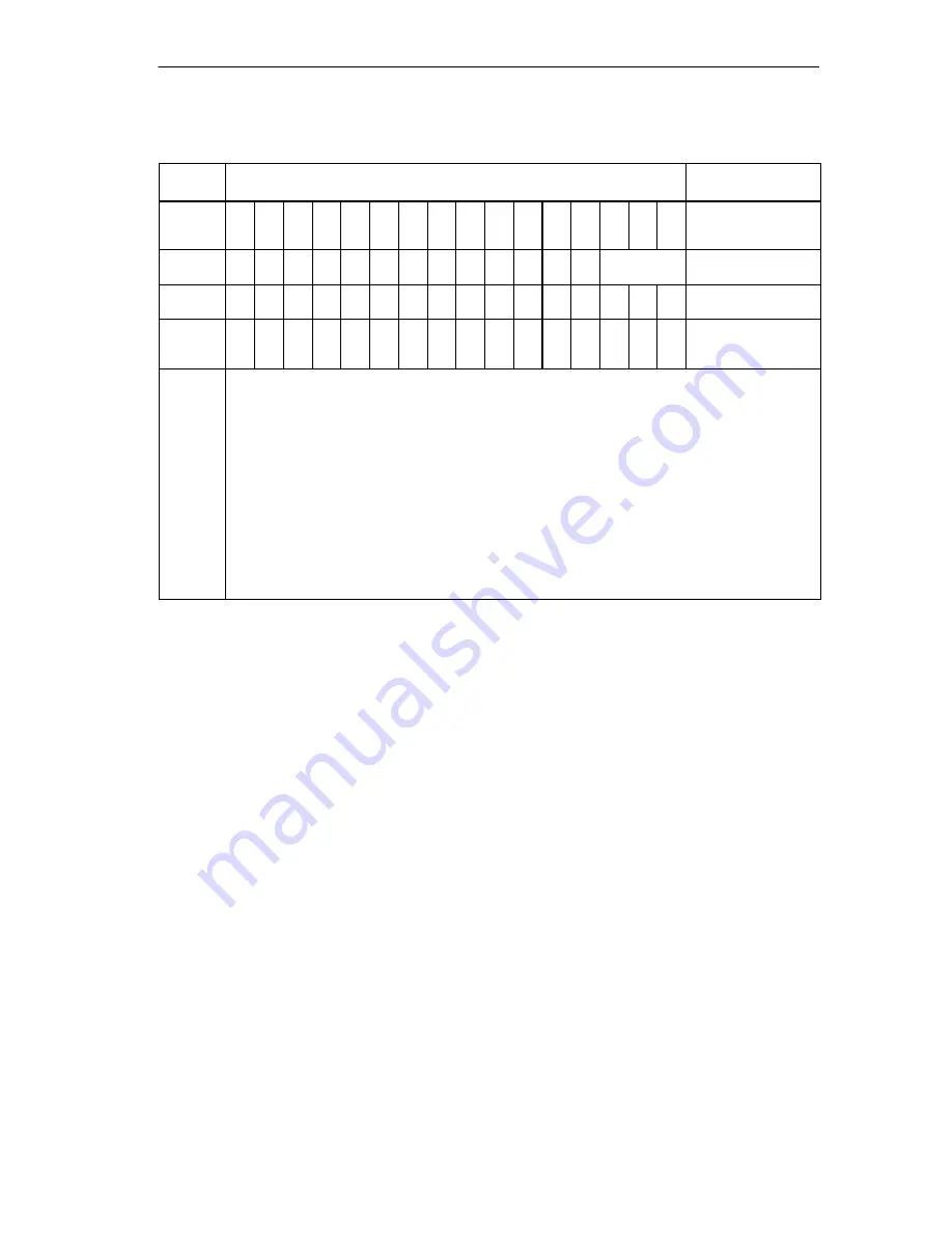
Meaning of the Control Bits in the Analog Input Function (IF 961-AIO)
Offset
Address
D15
Writing
D0
Remark
08
H
A
C
I
N
T
0
0
0
0
0
0
0
0
0
0
0
ta
ta
ta
Control register 1
0A
H
0
0
0
0
0
0
0
0
0
0
0
0
0
ADC
channel no.
Control register 2
0C
H
0
0
0
0
0
0
0
0
0
0
0
0
0
0
0
S
C
Status register ADC
0E
H
x
x
x
x
x
x
x
x
x
x
x
x
x
x
x
x
Acknowledge
interrupt
x = any
ta = 000
ta = 001
ta = 010
ta = 011
ta = 100
AC = 1
INT = 1
ADC channel no.
ADC = 001
ADC = 010
ADC = 011
ADC = 100
SC = 1
5.7 ms cycle time of the automatic conversion function
2.8 ms
1.3 ms
600
µ
s
185
µ
s
Automatic conversion of all ADC channels active
Generation of an interrupt after end of cycle
Number of the selected ADC channel:
channel 0
channel 1
channel 2
channel 3
Start of analog-digital conversion, (SC = Start of conversion in the case of individual
encoding)
Status After Switching On
Control register 1:
AC = 0, INT = 0, ta = 0
⇒
5.7 ms
Control register 2:
ADC = 001
⇒
ADC channel no. = 0
Status register ADC:
SC = 0
Individual Start of an ADC Channel
Below are listed the steps required for individual encoding in the case of an ADC
channel:
1. Select the ADC input channel by writing the channel number into control register
2 (offset address “0A
H
”).
2. Start the ADC conversion by setting the SC bit in the status register ADC to “1”
(offset address “0C
H
”).
3. Read bit “EOC” in the status register ADC at offset address (0C
H
) and wait until
EOC = 1.
4. Read the analog value at the relevant address (offset addresses “00
H
” to “06
H
”).


