- 75 -
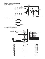
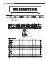
IC BLOCK DIAGRAM & DESCRIPTION
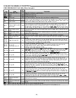
P3
0
- P3
3
I/O port P3
I/O
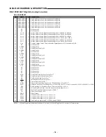
P30 functions as an input pin of RDY; and P31, P32. P33 function as the output pins of RD,
BLW, BHW, respectively. P30 also functions as an I/O port pin according to the resister
setting. When the external data has a width of 8 bits, be BHW pin functions
P4
0
- P4
7
I/O port P4
I/O
P4
0
- P4
4
function as output or input pins of ALE, ø1, HLDA, HOLD, CS
0
, and P4
5
- P4
7
as
I/O port pins, respectively. According to the resister setting, P4
0
- P4
3
also function as I/O port
pins, and P4
5
- P4
7
as output pins of CS
1
- CS
3
.
P5
0
- P5
7
I/O port P5
I/O
Port P5 is an 8-bit I/O port. This port has an I/O direction resister, and each pin can be
programmed for input or output. These pins enter the input mode at reset. These pins also
function as I/O pins for timers A0 - A3, output pins for the real-time output pins for the real-
time output, and input pins for the key-input interrupt.
P6
0
- P6
7
I/O port P6
I/O
Port P6 is an 8-bit I/O port. This port has an I/O direction resister, and each pin can be
programmed for input or output. These pins enter the input mode at reset. These pins also
function as I/O pins for timers A4, input pins for external interrupt inputs INT
0
- INT
2
, and input
pins for timers B0 - B2.
P7
0
- P7
7
I/O port P7
I/O
Port P7 is an 8-bit I/O port. This port has an I/O direction resister, and each pin can be
programmed for input or output. These pins enter the input mode at reset. These pins also
function as input pins for the A-D converter, output pins for the D-A converter, and input pins
for INT
2
, INT
3
, and INT
4
.
P8
0
- P8
7
I/O port P8
I/O
Port P8 is an 8-bit I/O port. This port has an I/O direction resister, and each pin can be
programmed for input or output. These pins enter the input mode at reset.
These pins also function as I/O pins for UART0, UART1, and input pins for INT
3
and INT
4
.
P10
0
/A
0
-
P10
7
A
7
Address (low-order)
output
Output Address (A
0
-A
7
) is output.
P11
0
/A
8
-
P11
7
/A
15
Address (middle-order)
output
Output
Address (A
8
-A
15
) is output. These pins also function as I/O port pins according to the resister
setting.
NMI
Non-mask able interrupt
Input
This pin is for a non-mask able interrupt.
Note : The X
IN
-input-clock division select bit is used to determine whether the input clock to pin X
IN
is to be divided or not.
Pin
Name
Input/O
utput
Description
V
CC
,V
SS
Power supply input --- Apply 5V ± 0.5V to Vcc, and 0V to Vss.
MD0
MD0
Input
Connect this pin to Vcc.
MD1
MD1
Input
Connect this pin to Vss.
RESET
Reset input
Input
The microcomputer is reset when Vss-level voltage is applied to this pin.
X
IN
Clock input
Input
X
OUT
Clock output
Output
BYTE
External data bus width
select input
Input
This pin determines whether the external data bus has an 8-bit width or 16-bit width for the
memory expansion mode or microprocessor mode. The width is 16 bits when V
SS
-level
voltage is input, and 8 bits when V
CC
-level voltage is applied. When BYTE=V
SS
level, by the
resister setting, the external data bus for each of areas CS
1
to CS
3
can have a width of 8 bits.
CDSEL
Clock division select
input
Input
This pin determines the X
IN
-input-clock division select bit's (note) state at reset and the input
level at pin X
IN
.
AV
CC
,
AV
SS
Analog power supply
input
---
Power supply input pins for the A-D converter and the D-A converter. Connect AV
CC
to V
CC
,
and AV
SS
to V
SS
externally.
V
REF
Reference voltage input
Input
This is the reference voltage input pin for the A-D converter and the D-A converter.
P0
0
/A
16
-
P0
7
/A
23
Address (high-order)
output
Output
Address (A
16
-A
23
) is output. These pins also function as I/O port pins according to the resister
setting.
P1
0
/D
0
-
P1
7
/D
7
Data (low-order) I/O
I/O
The low-order 8 bits of data (D
0
-D
7
) are input /output. When the external data bus has an 8-
bit width, address (LA
0
-LA
7
) output and data (D
0
-D
7
) input/output can be performed with the
time-sharing method, according to the resister setting.
P2
0
/D
8
-
P2
7
/D
15
I/O port p2,
Data (high-order) I/O
I/O
■
When 8-bit external data bus is used.
Port P2 is an 8-bit I/O port. This port has an I/O direction resister, and each pin can be
programmed for input or output. These pins enter the input mode at reset.
■
When 16-bit external data bus is used.
The high-order 8 bits of data (D
8
- D
15
) are input or output.
These are input and output pins of the internal clock generating circuit. Connect a ceramic or
quartz-crystal resonator between the X
IN
and X
OUT
pins. When an external clock is used., the
clock source should be connected to the X
IN
pin, and the X
OUT
pin s
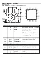
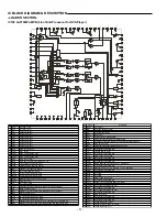
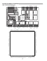
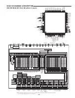
IC500 M37903S4CHP (16-bit C-Mos Micro Computer)
Summary of Contents for AVD-8501
Page 8: ... 7 MEMO ...
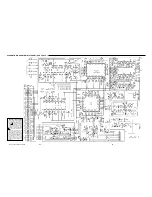
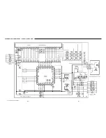
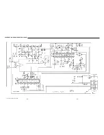
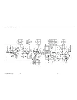
Page 65: ... 85 84 SCHEMATIC DIAGRAM MPEG This is a basic schematic diagram ...
Page 67: ... 115 114 SCHEMATIC DIAGRAM FRONT LED SW FOR UK XE This is a basic schematic diagram ...
Page 68: ... 119 118 SCHEMATIC DIAGRAM TUNER FOR UK XE This is a basic schematic diagram ...
Page 69: ... 121 120 This is a basic schematic diagram SCHEMATIC DIAGRAM FRONT LED SW FOR SS AU ...
Page 70: ... 125 124 This is a basic schematic diagram SCHEMATIC DIAGRAM TUNER FOR SS AU ...
Page 71: ... 127 126 SCHEMATIC DIAGRAM VIDEO FOR US CA This is a basic schematic diagram ...
Page 72: ... 131 130 SCHEMATIC DIAGRAM VIDEO FOR UK XE This is a basic schematic diagram ...
Page 73: ... 135 134 SCHEMATIC DIAGRAM VIDEO FOR SS AU This is a basic schematic diagram ...
Page 75: ...SANYO Electric Co Ltd Osaka Japan Aug 01 3950 BB Printed in Japan ...
Page 83: ... 33 32 MPEG P W BOARD SCHEMATIC DIAGRAM FOR WAVEFORM CHECK This is a basic waveform check ...
Page 84: ... 81 80 WIRING DIAGRAM MPEG A SIDE ...
Page 85: ... 83 82 WIRING DIAGRAM MPEG B SIDE ...
Page 86: ... 89 88 WIRING DIAGRAM MAIN FOR US CA ...
Page 90: ... 97 96 WIRING DIAGRAM MAIN FOR UK XE ...
Page 92: ... 101 100 WIRING DIAGRAM MAIN FOR SS ...
Page 94: ... 105 104 WIRING DIAGRAM MAIN FOR AU ...
Page 96: ... 109 108 SCHEMATIC DIAGRAM FRONT LED SW FOR US CA This is a basic schematic diagram ...
Page 97: ... 111 110 SCHEMATIC DIAGRAM TUNER FOR US CA This is a basic schematic diagram ...
Page 101: ... 129 128 WIRING DIAGRAM VIDEO FOR US CA ...
Page 102: ... 133 132 WIRING DIAGRAM VIDEO FOR UK XE ...
Page 103: ... 137 136 WIRING DIAGRAM VIDEO FOR SS AU ...
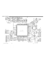
Page 104: ... 139 138 SCHEMATIC DIAGRAM DVD This is a basic schematic diagram ...
Page 105: ... 141 140 SCHEMATIC DIAGRAM DVD TOP LEFT This is a basic schematic diagram ...
Page 106: ... 143 142 SCHEMATIC DIAGRAM DVD BOTTOM LEFT This is a basic schematic diagram ...
Page 107: ... 145 144 SCHEMATIC DIAGRAM DVD TOP RIGHT This is a basic schematic diagram ...
Page 108: ... 147 146 SCHEMATIC DIAGRAM DVD BOTTOM RIGHT This is a basic schematic diagram ...
Page 109: ... 148 WIRING DIAGRAM DVD A SIDE ...
Page 110: ... 149 WIRING DIAGRAM DVD B SIDE ...


