- 63 -
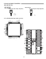
IC BLOCK DIAGRAM & DESCRIPTION
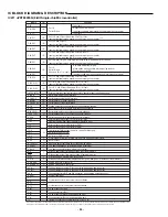
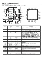
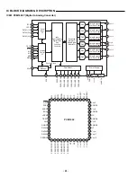
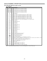
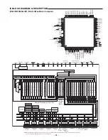
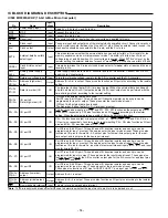
IC601 uPD16311GC-AB6 (1/8 to 1/16-Duty FIP(VFD) Controller/Driver
-FRONT SECTION-
6
5
8
9
52
10~13
27~32
35,36
1~4
50
46
14,33,45
51
34
37
44
26
15
D
IN
CLK
STB
OSC
Key
1
to
Key
4
SW
1
to
SW
4
D
OUT
LED
1
LED
5
V
DD
(+5V)
V
SS
(0V)
V
EE
(-30V)
Seg
1
Seg
12
Seg
13
/Grid
16
Seg
20
/Grid
9
Grid
1
Grid
8
OSC
Serial
I/F
Command decoder
Dimming
circuit
Display memory
20 bitx16 word
Timing generator
key scan
Key data
memory (4x12)
5-bit latch
18-bit shift register
20-bit outpur latch
4-bit latch
Segment dr
iv
er
Segment/g
ri
d
dr
iv
er
Gr
id dr
iv
er
Data selector
1
2
3
4
5
6
7
8
9
10
11
12
13
39
38
37
36
35
34
33
32
31
30
29
28
27
51
52
50 49 48 47 46 45 44 43 42
40
41
14 15 16 17 18 19 20 21 22 23 24
26
25
SW
1
SW
2
SW
3
SW
4
D
OUT
D
IN
IC
CLK
STB
KEY
1
KEY
2
KEY
3
KEY
4
Grid
6
Grid
7
Grid
8
Seg
20
/Grid
9
Seg
19
/Grid
10
V
EE
V
DD
Seg
18
/Grid
11
Seg
17
/Grid
12
Seg
16
/Grid
13
Seg
15
/Geig
14
Seg
14
/Grid
15
Seg
13
/Grid
16
OSC
V
SS
LED
1
LED
2
LED
3
LED
4
LED
5
V
DD
Gr
id
1
Gr
id
2
Gr
id
3
Gr
id
4
Gr
id
5
V
DD
Seg
1
/KS
1
Seg
2
/KS
2
Seg
3
/KS
3
Seg
4
/KS
4
Seg
5
/KS
5
Seg
6
/KS
6
Seg
7
/KS
7
Seg
8
/KS
8
Seg
9
/KS
9
Seg
10
/KS
10
Seg
11
/KS
11
Seg
12
/KS
12
Pin No.
Pin Name
Symbol
Description
6
5
9
8
52
15 to 26
44 to 37
27 to 32
35 to 36
50 to 46
10 to 13
1 to 4
14,33,45
51
34
7
D
IN
D
OUT
STB
CLK
OSC
Seg
13
/Grid
16
to
Seg
20
/Grid
9
Seg
1
/KS
1
to
Seg
12
/KS
12
Grid
1
to Grid
8
SW
1
to SW
4
Key
1
to Key
4
LED
1
to LED
5
V
DD
V
SS
V
EE
IC
Data input
Data output
Strobe
Clock input
LED output
Key data intput
Switch intput
Logic power
Internally connected
Logic ground
Pull-down level
Oscillator pin
High-voltage output
(segment)
High-voltage output
(segment/grid)
High-voltage output (grid)
Inputs serial data at rising edge of shift clock, starting from lower
bit.
Outputs serial data at falling edge of shift clock, starting from lower
bit. This is N-ch open-drain output pin.
Initializes serial interface at rising or falling edge to make
µ
PD16311 waiting for reception of command. Data input after
STB has fallen is processed as command. While command data
is processed, current processing is stopped, and serial interface
is initialized.While STB is high, CLK is ignored.
Reads serial data at rising edge, and outputs data at falling edge.
Connect resistor for determining oscillation frequency to this pin.
Segment output pins (Dual function as key source).
Grid output pins.
These pins are selectable for segment or grid output.
CMOS output. +20 mA max.
Data input to these pins is latched at end of display cycle.
These pins constitute 4-bit general-purpose input port.
5V–10%
Connect this pin to GND of system.
V
DD
- 35V max.
Be sure to leave this pin open (this pin is at V
DD
level).
Summary of Contents for AVD-8501
Page 8: ... 7 MEMO ...
Page 65: ... 85 84 SCHEMATIC DIAGRAM MPEG This is a basic schematic diagram ...
Page 67: ... 115 114 SCHEMATIC DIAGRAM FRONT LED SW FOR UK XE This is a basic schematic diagram ...
Page 68: ... 119 118 SCHEMATIC DIAGRAM TUNER FOR UK XE This is a basic schematic diagram ...
Page 69: ... 121 120 This is a basic schematic diagram SCHEMATIC DIAGRAM FRONT LED SW FOR SS AU ...
Page 70: ... 125 124 This is a basic schematic diagram SCHEMATIC DIAGRAM TUNER FOR SS AU ...
Page 71: ... 127 126 SCHEMATIC DIAGRAM VIDEO FOR US CA This is a basic schematic diagram ...
Page 72: ... 131 130 SCHEMATIC DIAGRAM VIDEO FOR UK XE This is a basic schematic diagram ...
Page 73: ... 135 134 SCHEMATIC DIAGRAM VIDEO FOR SS AU This is a basic schematic diagram ...
Page 75: ...SANYO Electric Co Ltd Osaka Japan Aug 01 3950 BB Printed in Japan ...
Page 83: ... 33 32 MPEG P W BOARD SCHEMATIC DIAGRAM FOR WAVEFORM CHECK This is a basic waveform check ...
Page 84: ... 81 80 WIRING DIAGRAM MPEG A SIDE ...
Page 85: ... 83 82 WIRING DIAGRAM MPEG B SIDE ...
Page 86: ... 89 88 WIRING DIAGRAM MAIN FOR US CA ...
Page 90: ... 97 96 WIRING DIAGRAM MAIN FOR UK XE ...
Page 92: ... 101 100 WIRING DIAGRAM MAIN FOR SS ...
Page 94: ... 105 104 WIRING DIAGRAM MAIN FOR AU ...
Page 96: ... 109 108 SCHEMATIC DIAGRAM FRONT LED SW FOR US CA This is a basic schematic diagram ...
Page 97: ... 111 110 SCHEMATIC DIAGRAM TUNER FOR US CA This is a basic schematic diagram ...
Page 101: ... 129 128 WIRING DIAGRAM VIDEO FOR US CA ...
Page 102: ... 133 132 WIRING DIAGRAM VIDEO FOR UK XE ...
Page 103: ... 137 136 WIRING DIAGRAM VIDEO FOR SS AU ...
Page 104: ... 139 138 SCHEMATIC DIAGRAM DVD This is a basic schematic diagram ...
Page 105: ... 141 140 SCHEMATIC DIAGRAM DVD TOP LEFT This is a basic schematic diagram ...
Page 106: ... 143 142 SCHEMATIC DIAGRAM DVD BOTTOM LEFT This is a basic schematic diagram ...
Page 107: ... 145 144 SCHEMATIC DIAGRAM DVD TOP RIGHT This is a basic schematic diagram ...
Page 108: ... 147 146 SCHEMATIC DIAGRAM DVD BOTTOM RIGHT This is a basic schematic diagram ...
Page 109: ... 148 WIRING DIAGRAM DVD A SIDE ...
Page 110: ... 149 WIRING DIAGRAM DVD B SIDE ...

