Samsung Electronics
6-3
PCB Diagram
6-2 MAIN PCB Bottom
No.
Description
1
MEMORY IC
- Supports data storage and transfer in
the system.
2
LCD Connector
- Connects and holds the LCD in position
3
Finger GASKET
- Improved resistance to ESD
4
26MHz Crystal
- Bluetooth CLK
5
Bluetooth IC
- Controls Bluetooth features
6
Touch PAD Connector
- Insert from the side.
- Connect the PCB and the touch pad
using the FPCB.
7
Earphone Jack
8
USB Connector
- Cable port for communication with
external devices
9
MIC
- Supports voice recording
0
Main IC
(ARM1176 Core, 600MHz, RTC module
are built in)
- Controls overall system functions
!
Mobile DDR SDRAM IC
- Supports data transfer in the system
@
PM IC
- Battery charger and dual buck
converter are built in
#
Battery connector
- Connects and holds the battery in
position
$
Finger GASKET
- Improved resistance to ESD
1
2
3
5
4
6
7
8
9
0
!
@
#
$
TP4
TP2
TP6
TP3
TP6
TP6
TP7
CON901
CON601
CON802
CON801
U503
U502
U301
U102
U601
U501
Summary of Contents for YP-R1
Page 15: ...3 4 Samsung Electronics MEMO ...
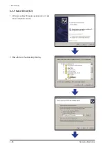
Page 44: ...Samsung Electronics 4 29 Troubleshooting Install completed Check device manager ...
Page 48: ...MEMO Samsung Electronics 4 33 ...
Page 53: ...5 5 Samsung Electronics MEMO ...
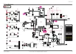
Page 58: ...Samsung Electronics 6 5 PCB Diagram 6 2 2 Test Point Wave Form TP2 TP3 TP4 TP7 TP6 ...
Page 59: ...6 6 Samsung Electronics MEMO ...
Page 69: ...7 10 Samsung Electronics MEMO ...


