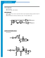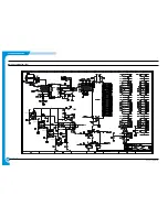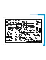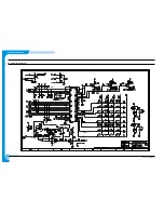
CIRCUIT DESCRIPTION
3.2 OPE
3.2.1 Basic Concept
3.2.2 UART Operation
3.2.1.1 Overview
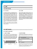
OPE BOARD is separated from the Main Board functional-
ly, and operates entire Micom(HT48C5A-000Z) in the
Board. OPE and Main exchange mutual information using
UART(universal asynchronous receiver/transmitter) chan-
nel. Also, Resetting of OPE is designed to control at the
Main. Micom in OPE performs key-scanning and LCD, LED
display control, and senses document detect, Scan position
and so on. When information is generated from OPE(key
touch, sensor level change, etc.), it sends specific code
coping with the situation to Main, and the Main operates
system by analyzing this code. If the Main tries to display
data on OPE, the Main sends data to OPE via UART line
on the basis of the format specified, and OPE displays it to
LCD.
In the case of the TAD Model, the MIC for the Speaker
Phone and OGM and the Pre-Amp part of the MIC have
built-in at OPE circuit.
3.2.1.2 UART
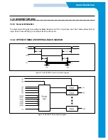
OPE and MAIN exchange information mutually by using
asynchronous communication mode(UART), and in full
duplex. Band rate is 9600bps, and uses 7.37MHz resonator
as oscillating element. It engages in communication with
8bit data without parity bit. UART line has two lines for Tx
and Rx, and the default level is in the 'high' state. For com-
munication, the start bit(low level) is transmitted before 8bit
data. When the data transmission(8bit) is completed, the
high state is maintained as the stop bit(high level) is trans-
mitted. Data is transmitted from LSB(DO), and MSB(D7) is
transmitted lastly.
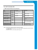
3.2.2.1 UART Communication
<1> UART TX FORMAT
Codes for change of KEY, TOUCH, SENSOR LEVEL and
so on are transmitted in single code without PRE/POST
DATA, and OK or Error messages to check if communica-
tion is performed properly are also transmitted in single
code. Provided that, in case the Main requested a certain
value(LCD, other register) particularly, data requested is
transmitted followed by sending Post Data('EOH') first.
<2> UART RX FORMAT
Data being received will be arranged to be received accord-
ing to the following specified format to know what data they
are.
DATA are received in the sequence of A,B,C, and D, and
the Check sum to check if the transmission is made prop-
erly will be found by doing XOR data from A to C.
a)
Type of data received
b)
Number of data (N+1) received after.
----------
c) DATA(N)
----------
d) Check
sum(1)
start
stop
bit
data 8bit (D0 ~ D7)
bit
D0
D1
D2
D3
D4
D5
D6
D7
Summary of Contents for SF-335T
Page 2: ......
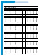
Page 19: ...CIRCUIT DESCRIPTION 2 Chorus 2 Assigned GPO Ports for RHINE ...
Page 21: ...CIRCUIT DESCRIPTION 5 HP IMPORTANT ASIC Ports for RHINE ...
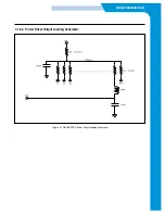
Page 24: ...CIRCUIT DESCRIPTION 3 1 5 3 Block Diagram Figure 16 Block Diagram of IP_TOP ...
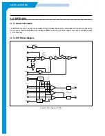
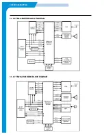
Page 35: ...CIRCUIT DESCRIPTION 3 1 8 6 FM214 MODEM BLOCK DIAGRAM 3 1 8 7 FM214 VS MODEM BLOCK DIAGRAM ...
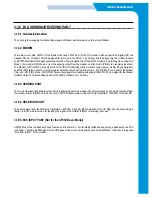
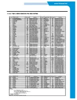
Page 36: ...CIRCUIT DESCRIPTION 3 1 8 8 FM214 SERIES MODEM PIN DESCRIPTION ...
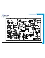
Page 48: ...4 5 Samsung Electronics SCHEMATIC DIAGRAMS Repair Manual 4 2 LIU Circuit Diagram 2002 06 25 ...

