CIRCUIT DESCRIPTION
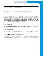
3.1.3.3 RESET circuit
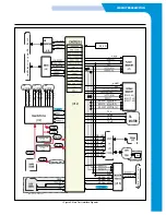
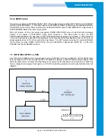
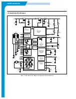
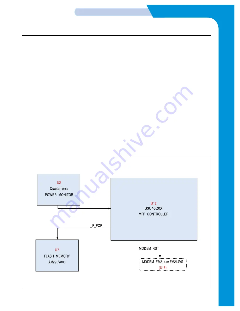
This system is configured with PRIMARY RESET(_RST) of Power Reset, Reset by WATCH DOG TIMER, external PRIMARY
RESET, and SECOND RESET(__F_POR) which was done AND. PRIMARY RESET SYSTEM is used for resetting MAIN CON-
TROLLER(U12) when System Power is authorized, and SECOND RESET resets FLASH MEMORY(U7). Figure below is
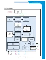
BLOCK DIAGRAM related to the reset of entire system.
When +5V r4.75V so that system may operate, POWER MONITOR(U2) moves to High(+5V) after maintaining
low(OV) in the degree of 50mS-200mS output while monitoring it. This Reset signal is input into MFP
CONTROLLER(S3C46Q0X, U12) right away, and MFP CONTROLLER becomes awake. And it releases _F_POR after MCLK
1 clock. The Quarter-horse needs +24V to be operated, but +5.0V is supplied by the Buck Regulator circuit. If +5.0V is incom-
pletely supplied such as +4.75V, it is checked as the Power Failure. The _RST output becomes low (0V), and the S3C46Q0X
(U12) confirms it to make it RESET (LOW ACTIVE). When the S3C46Q0X is released from RESET, the _F_POR of the
S3C46Q0X and FLASH MEMORY are reset.
<1> WATCH DOG OUTPUT (_F_POR)
Since WATCH DOG TIMER, which is Programmable Counter in (S3C46Q0X, U12) is set as disable for INITIAL STATE, it shall
be set as Disable so that it won’t operate, and after it is initialized for operation, it shall be reused by setting it Enable. When
Watch Dog Reset occurs, it is about 10mS depending on the value set at the initial stage. And Counter value of Watch Dog
Timer is changed by the program. Reset signal (_F_POR,U12-94) shall be generated, and entire system shall be Reset and
initialized.
_RST
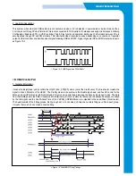
< Figure 13. POWER RESET BLOCK DIAGRAM >
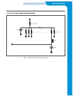
Summary of Contents for SF-335T
Page 2: ......
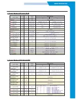
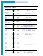
Page 19: ...CIRCUIT DESCRIPTION 2 Chorus 2 Assigned GPO Ports for RHINE ...
Page 21: ...CIRCUIT DESCRIPTION 5 HP IMPORTANT ASIC Ports for RHINE ...
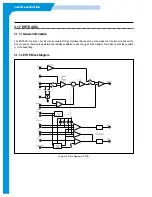
Page 24: ...CIRCUIT DESCRIPTION 3 1 5 3 Block Diagram Figure 16 Block Diagram of IP_TOP ...
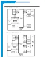
Page 35: ...CIRCUIT DESCRIPTION 3 1 8 6 FM214 MODEM BLOCK DIAGRAM 3 1 8 7 FM214 VS MODEM BLOCK DIAGRAM ...
Page 36: ...CIRCUIT DESCRIPTION 3 1 8 8 FM214 SERIES MODEM PIN DESCRIPTION ...
Page 48: ...4 5 Samsung Electronics SCHEMATIC DIAGRAMS Repair Manual 4 2 LIU Circuit Diagram 2002 06 25 ...

