58
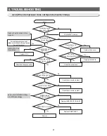
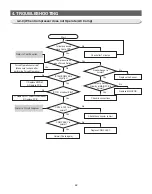
4. TROUBLESHOOTING
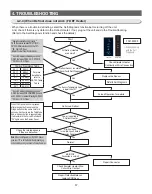
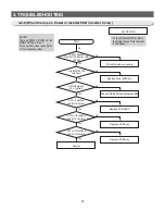
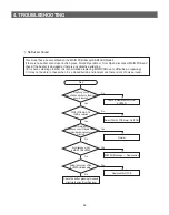
Is 230V applied
at both of the Inverter PCB
CN102?
Is the INVERTER PCB
Fuse blown?
Is DC320V applied to
BD1+/- terminals?
Is DC 5.8V
applied between TOP S/W
Top245P C-S (C104)?
Is 12V applied to
both of C106 terminals?
Is 5V applied to
both of C108 terminals?
Does PANEL PCB
operate normally?
Do Relays operate normally?
Is there any short
or breakage on PCB
Soldering?
Start
Normal
Check the wire connectors
Replace Fuse (250V 5A)
Check PCB Pattern and Replace BD1
Replace PCB ASS'Y
1) Replace D103 (RK49)
2) Replace PCB ASS'Y
Replace REG1 (7805)
1) Check the Wire Connection
and correct it if necessary
2) Replace PANEL PCB
- Check MAIN PCB Connectors
- Check Wire Connection between
CABI and DOOR
- Check DOOR PANEL PCB
Connection
1) Repair Related Parts or
Replace PCB
No
No
No
No
No
No
No
Yes
No
Yes
Yes
Yes
Yes
Yes
Yes
Yes
Yes
No
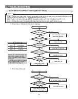
Caution
There is AC230V or DC300V at the
MAIN PCB Power Circuit.
So, be cautious when repairing the
unit or measuring values.
- To check the MAIN PCB, refer to
the Operation and 'Refer' sections
in this manual
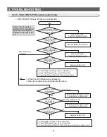
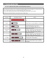
4-2-5) When there is no Power in Inverter PCB (Inverter Comp )
G/H/L/P/R/Z Option
Summary of Contents for RL60GG Series
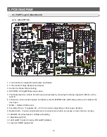
Page 75: ...75 5 PCB DIAGRAM 5 3 Connector Layout and Description Main Board 5 3 1 Q G J OPTION...
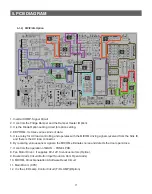
Page 76: ...76 5 PCB DIAGRAM 5 3 2 R P Z H Option...
Page 77: ...77 5 PCB DIAGRAM 5 3 3 L Option...
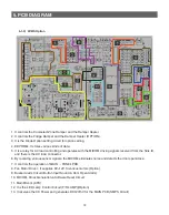
Page 78: ...78 5 PCB DIAGRAM 5 3 4 W E Option...
Page 80: ...80 5 PCB DIAGRAM IPM DIODE VOLTAGE 5 5 IPM Diode Voltage...
Page 81: ...81 6 WIRING DIAGRAM 6 1 Q G J OPTION...
Page 82: ...82 6 WIRING DIAGRAM 6 2 R P Z H Option...
Page 83: ...83 6 WIRING DIAGRAM 6 3 L Option...
Page 84: ...84 6 WIRING DIAGRAM 6 4 W E Option...
Page 85: ...85 6 WIRING DIAGRAM 6 5 S Option...
Page 86: ...86 7 CIRCUIT DIAGRAM 7 1 Schematic Diagram PBA Main 7 1 1 Q G J OPTION...
Page 87: ...87 7 CIRCUIT DIAGRAM 7 1 2 R P Z H L Option...
Page 88: ...88 7 CIRCUIT DIAGRAM 7 1 3 W E S Option...
Page 89: ...89 7 CIRCUIT DIAGRAM 7 2 Schematic Diagram PBA Inverter...
Page 90: ...90 7 CIRCUIT DIAGRAM 7 3 Block Diagram PBA Main...
Page 91: ...91 7 CIRCUIT DIAGRAM 7 4 Block Diagram PBA Inverter G H L P R Z Option...
Page 92: ...92 7 CIRCUIT DIAGRAM 7 5 Block Diagram PBA Inverter Q J Option...


