background image


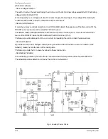
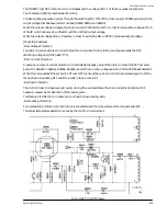
Fig. 18. Chopper Circuit 


6-

22

Samsung Electronics

Circuit Operation Description

Summary of Contents for D61B

Page 1: ...nformation Specifications Introduction PDP Alignment and Adjustments Troubleshooting Circuit Description Handling Description Glossary Schematic Diagrams 1 2 3 4 5 6 7 8 9 10 P L A S M A D I S P L AY T V PLASMA DISPLAY TV Chassis D61B ...

Page 2: ...g Electronics Co Ltd Mar 2004 Printed in Korea AA82 01375A This Service Manual is a property of Samsung Electronics Co Ltd Any unauthorized use of Manual can be punished under applicable International and or domestic law ...

Page 3: ...rectly into the power outlet With the unit s AC switch first in the ON position and then OFF measure the current between a known earth ground metal water pipe conduit etc and all exposed metal parts including antennas handle brackets metal cabinets screwheads and control shafts The current measured should not exceed 3 5 milliamp Reverse the power plug prongs in the AC outlet and repeat the test Fi...

Page 4: ...ondary ground system in addition to the main chassis ground This secondary ground system is not isolated from the AC power line The two ground systems are electrically separated by insulating material that must not be defeated or altered 13 Components parts and wiring that appear to have overheated or that are otherwise damaged should be replaced with parts that meet the original specifications Al...

Page 5: ...o the unit or any of its assemblies unless all solid state heat sinks are correctly installed 7 Always connect a test instrument s ground lead to the instrument chassis ground before connecting the positive lead always remove the instrument s ground lead last 8 Plasma display panels have partial afterim ages when a same picture continues to be dis played for a certain time This happens due to the ...

Page 6: ...oldering iron when soldering or unsoldering ESDs 6 Use only an anti static solder removal device Many solder removal devices are not rated as anti static these can accumulate sufficient electrical charge to damage ESDs 7 Do not remove a replacement ESD from its protective package until you are ready to install it Most replacement ESDs are packaged with leads that are electrically shorted together ...

Page 7: ...rtz Hour Inches Per Second Kilowatt hour Kilogram Kilohertz Kilohm Kilometer Kilometer Per Hour Kilovolt Kilovolt ampere Kilowatt Liter Megahertz MV MW MΩ m µA µF µH µm µs µW mA mg mH mI mm ms mV nF Ω pF Ib rpm rps s V VA W Wh Megavolt Megawatt Megohm Meter Microampere Microfarad Microhenry Micrometer Microsecond Microwatt Milliampere Milligram Millihenry Milliliter Millimeter Millisecond Millivol...

Page 8: ...afe Ground Green Y High High Frequency High Fidelity Inductance Capacitance Integrated Circuit Intermediate Frequency I O L L LED LF MOSFET MTS NAB NEC NTSC OSD PCB PLL PWM QIF R RC RF R Y SAP SAW SIF SMPS S N SW TP TTL TV UHF UL UV VCD VCO VCXO VHF VIF VR VTR VTVM TR Input output Left Low Light Emitting Diode Low Frequency Metal Oxide Semiconductor Field Effect Tr Multi channel Television Sound N...

Page 9: ...x 79 D x 630 5 H mm 40 43 W x 3 11 D x 24 82 H inches 31 Kg 68 34 lbs without stand 107 Cm 42 Inches AC 120V 60Hz AC100 250V 50 60Hz 330 Watts 852 H X 480 V RS 232C IN Mini jack RS 232C OUT D SUB 9P VIDEO S VIDEO COMPONENT 1 COMPONENT 2 RGB PC 1 2 DVI External Speaker 10W 10W Audio Output L R RCA VIDEO S VIDEO COMPONENT 1 480i 480p 720p 1080i COMPONENT 2 RGB2 PC IN BNC 5P 480i 1080i VGA XGA RGB1 P...

Page 10: ...3 2 Samsung Electronics MEMO ...

Page 11: ...Bus electrode Dielectric ITO electrode MgO layer Barrier Phosphors Address Electrode Front panel Back panel 4 Introduction PDP 4 1 Cell Structure of PDP Samsung Electronics 4 1 Introduction PDP ...

Page 12: ... Y480 X X X A1 A2 A3 A4 A5 A6 A7 R e f e r e n c e A1 A2 Address Electrode Y1 Y2 Scan Sustain Electrode X Common Sustain Electrode 4 2 Electrode arrangement of SD PDP 4 2 Samsung Electronics Introduction PDP ...

Page 13: ...t emission from both side emission from both side AC AC PDP PDP V I V I Vf X Y Y X Making of Voltage Over Vf Y X Making of Voltage Over Vf Discharge Discharge Current Discharge Discharge Current X Y X Y Wall Charge Stop Discharge Wall Charge Stop Discharge 4 3 Discharge in AC PDP Samsung Electronics 4 3 Introduction PDP ...

Page 14: ...n are generated by collision Between accelerated Electron and neutrality particle Electron and Ion are generated by collision Between accelerated Electron and neutrality particle Many Electrons and Ions are generated continuously by collision It is end of first Discharge Many Electrons and Ions are generated continuously by collision It is end of first Discharge 4 4 Discharge Mechanism Process 4 4...

Page 15: ...icient of 2 nd electron emission Electron and ion are generated from 2 nd electron s acceleration and confliction Electron and ion are generated from 2 nd electron s acceleration and confliction Many Electrons and Ions are generated Continuously by collision Many Electrons and Ions are generated Continuously by collision 4 5 Discharge Mechanism Process Samsung Electronics 4 5 Introduction PDP ...

Page 16: ... pressure A function of an electrode distance Discharge Mechanism Delay Repeat of α process and β process Space insulation break down by increasing current Discharge Self sustained discharge Paschen Curve Start voltage of Discharge Vf Minimum voltage for discharge display a curve line of pressure A function of an electrode distance Discharge Mechanism Delay 4 6 Paschen Curve 4 6 Samsung Electronic...

Page 17: ...Wall Charge Vw1 Vex Vw1 X Y Discharge Start Discharge Start X Y Vex 0V 0V Y X Vex X Y X Y It is displayed differential discharge characteristics about same pulse by Wall Charge enable a picture V I Vf No Discharge No Discharge Vex Vw2 Vw2 X Y X Y ...

Page 18: ...l charge Make wall charge Input electric field Input electric field Discharge Discharge Sustain discharge Sustain discharge Extinction of discharge Wall charge Shield Make wall charge Extinction of discharge Wall charge Shield Make wall charge Input electric field Input electric field Discharge Discharge Sustain discharge Sustain discharge Introduction PDP ...

Page 19: ... Function Sustain Erase Wall Charge Set Issue Operation margin Contrast Short Time Function Select On Cell Issue H igh Speed L owV oltage L ow Failure Function Select On Cell Issue H igh Speed Low Voltage Low Failure Function D ischarge On Cell Issue High Efficiency L ow V oltage ERC Performance Function Discharge On Cell Issue H igh Efficiency Low Voltage ERC Performance 4 10 1 Sub field Precess ...

Page 20: ...4 10 Samsung Electronics 4 11 1Sub field Process Address 1 4 12 1Sub field Process Address 2 Introduction PDP ...

Page 21: ...Introduction PDP Samsung Electronics 4 11 4 13 1Sub field Process Address 3 4 14 1Sub field Process Address 4 ...

Page 22: ...Introduction PDP 4 12 Samsung Electronics 4 15 1Sub field Process Address 5 4 16 1Sub field Process Address 6 ...

Page 23: ...Introduction PDP Samsung Electronics 4 13 4 17 1Sub field Process Address 7 4 18 1Sub field Process Address 8 ...

Page 24: ...Introduction PDP 4 14 Samsung Electronics 4 20 1Sub field Process Sustain 4 19 1Sub field Process Address 9 ...

Page 25: ...sung Electronics 4 15 4 21 Frame Structure ADS SF1 SF2 SF3 SF4 SF5 SF6 SF7 SF8 1 2 480 128T 64T 32T 16T 8T 4T 2T 1T 1TV field time scan line address sustain sub field Reset Period Address Period Sustain Period X Y1 Y2 Yn D ...

Page 26: ...SF4 SF5 SF6 SF7 SF8 O r i g i n a l I m a g e 1 2 480 128T 64T 32T 16T 8T 4T 2T 1T 1TV field time scan line address sustain sub field Introduction PDP 4 22 Picture Structure by 8 sub field 4 16 Samsung Electronics ...

Page 27: ...ilure Address Pulse Scan Pulse potential difference Scan width a design High speed Addressing It is important technique for high resolution high brightness low cost Discharge delay reduction by discharge condition improvement and drive waveform Low voltage Address It is profitable of cost down by reduce resisting pressure Driver IC Sustain Period Pulse form Input alternation pulse to X electrode a...

Page 28: ...e Image Processing Processing Board Board Scan Buffer Board Scan Buffer Board Image signal source X Y C ontrol signal Address Data signal RGB Sync Cloc k Y output Scan power Scan signal Y output Scan P ulse X output Address output Port of Panel Electrode Port of Panel Electrode X Driver X Driver Board Board Input AC Power common in use Output All voltages of each B ds ...

Page 29: ...Introduction PDP Samsung Electronics 4 19 SMPS X BOARD PCB CONTROL Y BOARD DIGITAL BOARD LOGIC BOARD ANALOG BOARD 4 24 PCB ...

Page 30: ...4 20 Samsung Electronics MEMO ...

Page 31: ...n and enters service mode If you fail to enter service mode repeat steps 1 and 2 above 5 1 2 Initial DISPLAY State of SERVICE MODE 5 1 2 A OSD DISPLAY 5 1 2 B Button Operations in SERVICE MODE 1 VSP9437 1 9 CXA2101 2 VSP9437 2 10 LOSIC 3 FLI2300 11 TP LOG ASI 4 ASI500 1 12 Option 5 ASI500 2 13 CheckSum 0000 6 DNIe 14 Reset 7 AD9888 8 CXA2151 Release 2003 05 02 M_NNWS42M6_100 Menu UP DOWN Key LEFT ...

Page 32: ... AV 01 SECAM AV 27 NTSC AV 01 ASI II 500 DNIe Video PC DVI PI P R CONT 32 PI P G CONT 32 PI P B CONT 32 PI P R BRIGHT 00 PI P G BRIGHT 00 PI P B BRIGHT 00 PI P FILTERIC 00 PI P FILTER ML 00 PI P FILTER MR 00 PI P FILTER UC 00 BRIGHT OFFSET Attachment Attachment CONTRA OFFSET SCALE MAX Y 48 SCALE MIN Y 16 TH HPF 00 TH EDGE 04 05 NR SEL 02 CE UPPER 220 240 CE CUTOFF 45 CE GAIN 64 75 DCE GAIN 75 96 S...

Page 33: ... LC 00 FI LTER YPASS 00 R GAMMA 32 G GAMMA 32 B GAMMA 32 H POSITION 00 V POSITION 00 H SIZE 00 V SIZE 00 OVERSCAN R 50 OVERSCAN G 50 OVERSCAN B 50 AD9888 Vi deo Comp PC CXA2101 Vi deo COMP R GAI N 71 128 83 G GAI N 77 122 81 B GAI N 95 128 81 R OFFSET 63 79 64 G OFFSET 66 53 70 B OFFSET 64 82 68 V PATH PC AUTO COLOR OFF PICTURE 20 HUE 34 COLOR 19 BRIGHT 61 SHARPNESS 16 R DRI VE 04 G DRI VE 04 B DR...

Page 34: ...2 VSYNC WIDTH 02 HSYNC WIDTH 12 LOG PATTERN 00 LOG HIGH LEVEL 00 LOG LOW LEVEL 00 ASI COLORBAR 00 I C W B D ata V id e o S V H S C om p on e nt P C D V I D N Ie B r igh t 4 1 5 8 4 3 3 6 C o ntr ast 5 4 4 8 5 0 5 5 L o g ic R Ga in 1 4 9 1 4 5 1 5 3 1 4 5 G Gain 1 3 0 1 3 0 1 3 0 1 3 0 B Gain 1 2 5 1 1 9 1 1 3 1 1 7 R C uto ff 1 3 1 1 1 6 1 2 5 1 2 3 G C u to ff 1 3 0 1 2 7 1 2 8 1 2 8 B C uto ff ...

Page 35: ... At this time do not adjust the gain of AD9888 the Highlight W B does not need to be adjusted since its deviation falls within valid distribution range PC adjustment is same as DTV adjustment The offset can be applied to the values obtained through DTV adjustment However additional adjustment is required for Y Cb and Cr of DTV since PC processes R G and B signals cvbs adjustment is performed with ...

Page 36: ...ht measure point High Light measure point V id e o S V H S C o m p o n en t P C D V I T im ing 9 2 5 LTH P A L B 7 2 0 p 6 4 0 4 8 0 6 0 H z 6 4 0 4 8 0 6 0 H z H L x 2 7 5 2 8 0 2 8 0 2 8 0 y 2 8 0 2 8 7 2 9 5 2 9 5 Y fL 3 5 3 4 3 0 3 0 L L x 2 7 8 2 8 0 2 8 5 2 8 5 y 2 8 5 2 8 7 2 9 5 2 9 5 Y fL 1 3 0 6 0 8 0 8 ...

Page 37: ...PS Vs VSCAN VSET VA VE VSET VSCAN VE VA VS Adjust the S MPS voltage using the VR Variable Resistor Validate the SMPS voltage Not used by this Model Common use with Other Models S MPS Fan power source CN811 CN807 CN808 CN809 CN810 9 When the SMPS PCB is replaced the VA VSCAN VS VE and VSET voltages must be checked and adjusted to the proper to levels indicated on the panel sticker Notes ...

Page 38: ...Alignment and Adjustments 2 8 Samsung Electronics MEMO ...

Page 39: ...E 1 COMP1_Y1 2 GND 3 GND 4 COMP1_PB1 5 GND 6 COMP1_PR1 7 GND 8 CVBS_PAL 9 GND 10 SCL1 11 GND 12 SDA1 13 GND 14 GND CN102 NO PIN NAME 1 MUTE 2 VIDEO_OUT 3 GND 4 C_SUB 5 GND 6 CVBS_Y_SUB 7 GND 8 COMP2_Y2_G 9 GND 10 COMP2_PB2_B 11 GND 12 COMP2_PB2_R 13 GND 14 GND CN104 NO PIN NAME 1 CXA_Y 2 GND 3 CXA_CB 4 GND 5 CXA_CR 6 GND 7 CXA_HS 8 GND 9 CXA_VS 10 GND 11 PC_SL 12 PC_SR 13 GND 14 GND 1 ANALOG DIGIT...

Page 40: ...LKOut Rx CLKIn 2 GND 17 GND 3 Tx Out0 Rx In0 18 GND 4 Tx Out0 Rx In0 19 Tx Out3 Rx In3 5 GND 20 Tx Out3 Rx In3 6 GND 21 GND 7 Tx Out1 Rx In1 22 GND 8 Tx Out1 Rx In1 23 GND 9 GND 24 GND 10 GND 25 RESET_MN 11 Tx Out2 Rx In2 26 GND 12 Tx Out2 Rx In2 27 IIC SCL2 13 GND 28 GND 14 GND 29 IIC SDA2 15 Tx CLKOut Rx CLKIn 30 GND 31 GND ...

Page 41: ... 5 N C 6 GND 7 GND 8 D3 3V 9 D3 3V 10 GND 11 D6V CN801 CN802 Logic Pin no Power 1 D3 3V 2 D3 3V 3 GND 4 GND 5 D5V 6 GND 7 IC2 8 IC2 9 PS_ON 10 GND CN803 DC FAN Connector 1 2 3 4 Pin no Power 1 12V 2 GND 3 Fan_D CN807 CN811 CN812 Buffer 1 Pin no Power 1 Va 2 Va 3 N C 4 GND 5 GND CN804 X Drive Pin no Power 1 D5V 2 VG 3 GND 4 GND 5 VE 6 GND 7 GND 8 Vs 9 Vs CN805 Y Drive Pin no Power 1 D5V 2 VG 3 GND ...

Page 42: ...D 25 XF 11 XH 26 GND 12 GND 27 N C 13 XS 28 GND 14 GND 29 GND 15 XE 30 GND X LX2001 CN4005 Logic Pin no Signal Pin no Signal 1 N C 21 Yc 2 GND 22 GND 3 SIA 23 Yscan 4 GND 24 GND 5 CLK 25 Ysp 6 GND 26 GND 7 LE 27 Yp 8 GND 28 GND 9 STB 29 Ys 10 GND 30 GND 11 TSC 31 Yrr 12 GND 32 GND 13 START 33 YL 14 GND 34 GND 15 Ysc_c 35 Yg 16 GND 36 GND 17 Yf 37 Yfr 18 GND 38 GND 19 Yr 39 Yer 20 GND 40 Yh Y Y2001...

Page 43: ...B12 7 DOWN B9 32 DOWN R13 8 GND 33 DOWN G13 9 DOWN CLK BB1 34 DOWN B13 10 GND 35 GND 11 DOWN CLK B1 36 DOWN CLK A A1 12 GND 37 GND 13 DOWN R10 38 DOWN CLK A1 14 DOWN G10 39 GND 15 DOWN B10 40 N C 16 DOWN R11 41 N C 17 DOWN G11 42 N C 18 DOWN B11 43 N C 19 GND 44 N C 20 ERC09 45 N C 21 ERC10 46 N C 22 ERC11 47 A5V 23 ERC12 48 A5V 24 GND 49 A5V 25 DOWN BLK1 50 A5V LG2003 CN3300 Pin no Name Pin no Na...

Page 44: ...P G 21 31 UP R1 6 7 UP R21 32 UP B 17 8 GND 33 UP G17 9 UP CLK BB2 34 UP R1 7 10 GND 35 GND 11 UP C LK B2 36 UP CLK AA 2 12 GND 37 GND 13 UP B18 38 UP C LK A2 14 UP G 18 39 GND 15 UP R18 40 UP B 14 16 UP B19 41 UP G14 17 UP G 19 42 UP R1 4 18 UP R19 43 UP B 15 19 GND 44 UP G15 20 ERC5 45 UP R1 5 21 ERC6 46 N C 22 ERC7 47 A5V 23 ERC8 48 A5V 24 GND 49 A5V 25 UP BLK2 50 A5V SI3700 CN3611 Pin no Name ...

Page 45: ...31 UP R8 7 UP R13 32 UP B 9 8 GND 33 UP G9 9 UP CLK BB1 34 UP R9 10 GND 35 GND 11 UP C LK B1 36 UP CLK AA 1 12 GND 37 GND 13 UP B10 38 UP C LK A1 14 UP G 10 39 GND 15 UP R10 40 N C 16 UP B11 41 N C 17 UP G 11 42 N C 18 UP R11 43 N C 19 GND 44 N C 20 ERC5 45 N C 21 ERC6 46 N C 22 ERC7 47 A5V 23 ERC8 48 A5V 24 GND 49 A5V 25 UP BLK1 50 A5V LE2003 MS3701 Pin no Name Pin no Name 1 GND 26 UP POL2 2 UP B...

Page 46: ...Circuit Operation Description 6 8 Samsung Electronics 7 Y Addr Buf H Addr Buf E CN5013 Pin no Name 1 Vcc 2 Vcc 3 AGND 4 AGND CN5014 Pin no Name 1 Vcc 2 Vcc 3 AGND 4 AGND Y Addr Buf H Y Addr Buf E ...

Page 47: ...Main Power Block Diagram AC Input Sta nd by STR A6151 STD_5V 5V 0 46A PFC IC L4981A FET SPP20N 60C3 Di KCU20B60 D D 1 IC STR F6267 PS ON D5VL 5 3V 4 5A D3 4V IC NJM2374A TR 2SA1568 3 4V 5 2A Vg 15V 2 0A VT 33V 30 36V 0 006A A6V D6V 6V 2 0A A12V D12V 12V 2 0A 12V fa n 12V 8 12 1 0A Amp 12V or 18V D D 2 IC SP F9001 FET 2SK2698 Va 70V 60 85 3 0A Vscan 70V 60 80 0 3A Vset 150V 140 160 0 2A Ve 140V 130...

Page 48: ...Main Power Block Diagram AC Input Sta nd by STR A6151 STD_5V 5V 0 46A PFC IC L4981A FET SPP20N 60C3 Di KCU20B60 D D 1 IC STR F6267 PS ON D5VL 5 3V 4 5A D3 4V IC NJM2374A TR 2SA1568 3 4V 5 2A Vg 15V 2 0A VT 33V 30 36V 0 006A A6V D6V 6V 2 0A A12V D12V 12V 2 0A 12V fa n 12V 8 12 1 0A Amp 12V or 18V D D 2 IC SP F9001 FET 2SK2698 Va 70V 60 85 3 0A Vscan 70V 60 80 0 3A Vset 150V 140 160 0 2A Ve 140V 130...

Page 49: ... component reduces the line conducted external noise and the feedback noise from the power supply Fig 2 Input Filtering Circuit 2 Rectifier Circuit This component converts the inputincoming AC power into DC power Power Circuit Aux Power Circuit D8131 doesperforms the half wave rectification on the AC input and C8131 produces DC voltage with less ripple Main pPower cCircuit The Rrectified AC input ...

Page 50: ...hut down safely without smokinge or fire even when the inrush limit resistor heats up If this occurs replacement of R8103 and R8104 is required 4 Auxiliary Power Circuit Function Description By turning ON OFF the MOS FET inside the power control IC STR0A6151 the charged current is transferred from the electrolytic condenser C8131 to the secondary part to generate the output voltage for STD 5V the ...

Page 51: ...32 detects the current between the OCP terminal Pin 1 which is connected to the source of the MOSFET inside the STR A6151 and the GND terminal Pin 3 This feature prevents damage from the over current by regulating the current under the allowed load Overload Protection It provides UVLO Under Voltage Lockout during an overload status the drain current is limited by OCP behavior caused by a malfuncti...

Page 52: ...0 of the power factor Protection Features Over Voltage Protection The Voltage limiting type Over Voltage Protection feature limits the voltage under the set point and narrows the ON width of the FET while the hit occurs and the Overshoot or the no control by the load variation The set point value of the protection voltage is controlled by R8231 R8232 R8233 and R8234 Set the main power to around 44...

Page 53: ...es the input voltage the auxiliary power of the Vcc through the D8244 is applied to the IC STR F6267 and the oscillation begins The current runs through the primary coil R8301 of T8301 when the Internal MOSFET is ON The current climbs at the gradient specified by the value LR8301 converts the currents to voltage and Pin 1 of the IC detects it 6 14 Samsung Electronics Circuit Operation Description ...

Page 54: ...ge Vcc OVP 28V TYP Over Current Protection A pulse by pulse over current protection circuit detects the peak value of the drain current of the FET per every pulse The detection resistors R8301 RX8301 convert the current to voltage and Pin 2 of the STR F6267 detects it When this value exceeds the set point FET cuts OFF to cut out the current in order to be released again to ON by the next cycle Rep...

Page 55: ...ge increases The switching frequency increases and the interval to charge the resonance condenser C8338 shortens which results in limiting the output voltage Accordingly when the output voltage drops drawing the current from Pin 13 of the resonance IC which is not available the switching frequency drops and the interval to charge the resonance condenser lengthens resulting in increased output volt...

Page 56: ...6353 for Vscan and Vset STR A6351 for Ve packaging these IC have the same behavior The Vscan circuit is explained as an example When voltage is applied the voltage from the coil at Pins 11 16 of T8331 applies to the Vcc terminal Pin 4 of the IC When this voltage eaches the starting voltage the oscillation begins Samsung Electronics 6 17 Circuit Operation Description ...

Page 57: ...divided R8734 R8435 R8731 and R8736 When the output voltage increases the photocoupler PC8731 turns ON to increase the voltage at Pin 5 of the IC to narrow down the ON width for limited output voltage When the output voltage drops it reverses to widen the ON width for increased output voltage Protection Features Over Voltage Protection The Latch circuit is activated to stop the circuit when the Vc...

Page 58: ... Protection Features Over Voltage Protection The built in over voltage protection circuit is activated when the input voltage overruns Over Current Protection The built in over current protection circuit is activated around 2 1A Overheating Protection A built in overheating protection circuit is employed Fig 15 Dropper Circuit Samsung Electronics 6 19 Circuit Operation Description ...

Page 59: ...s 1 and 2 of the IC to output the variable 0 15V voltage and then L8041 C8042 rectify to drop the voltage The constant voltage regulation resistor divides the output voltage and is detected at Pin 4 of the IC Protection Features Over Current Protection The built in over current protection circuit is activated around 3 1A Overheating Protection A built in overheating protection circuit is employed ...

Page 60: ...o voltage and Pin 2 of the STR F6267 detects it When this value exceeds the set point the FET cuts OFF to cut out the current and is released to ON by the next cycle Repeating OFF and ON results in the current limit IC8001 SI 8050S has a built in over current protection circuit which is activated around 3 1A Overload Protection IC8301 STR F6267 performs UVLO Under Voltage Lockout during the overlo...

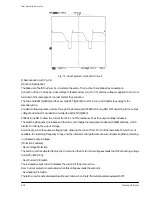
Page 61: ...Fig 18 Chopper Circuit 6 22 Samsung Electronics Circuit Operation Description ...

Page 62: ... and 46 4 Validate that data input is normal 656CLK Pins 4 195 13 5MHz HOUT Pin 1 15 75KHz VOUT Pin 2 60Hz 5 Validate that data output is normal S23CLK Pin 125 27MHz S23_HS Pin 119 31 5KHz S23_VS Pin 118 60Hz 6 Verify that the input output between FLI2310 and the MEMORY IC702 is normal 4 CXA2151Q Analog Board IC101 COMPONENT S W SYNC SEPARATION Check when the input mode is Component 1 2 High Defin...

Page 63: ... is delivered to ASI510 normally Digital R G B HSYNC VSYNC and CLK 4 Validate that data output is normal R G B digital data outputs RA801 RA806 SNI_HSYNC SNI_VSYNC and SNI_CLK 9 DNIe2 IC1003 PICTURE ENHANCER DNIe2 IC1003 PICTURE ENHANCER 1 Verify that the proper power is supplied 3 3V 1 8V 2 Validate that the pin RESET is LOW Pin 74 3 Validate the output of I2C BUS Pins 1 2 4 Verify that the outpu...

Page 64: ... Board Output Y Board Output SMPS CN801 802 Output Validate the AC input to SMPS CN800S SMPS LOGIC Board Change X Board Change Y Board Change PANEL Replace Display Board Change SMPS Fuse Abnormal Abnormal Abnormal Abnormal Abnormal Normal Normal Normal Normal Abnormal Abnormal Abnormal Abnormal 1 2 3 4 5 7 1 Partly no display ...

Page 65: ...ppear Cause Some buffer boards doesn t work correctly T rouble Shooting POWER ON Lower Part No Screen 1 2 No Screen Vertical 1 7 No Screen Vertical 3 4 No Screen Replace Lower Buffer board Replace Lower Sc an board Replace Address buffer board Replace PANEL No Replace Lower Buffer Board No 3 Replace Address buffer board 1 2 2 3 3 4 1 ...

Page 66: ...sn t exist on Screen Cause Fuse or FET is destroyed T rouble Shooting FUSE Y MAIN B OARD FET Y MAIN Check several points FUS E F5003 for Vs F5002 for Vcc F5001 for Vdd OPEN OK FET OK SHORT Y MAIN Normal State Replace the board Replace the board Q5009 Q5010 Q5012 Q5015 Q5017 Q5024 F5001 3 F5009 24 FUSE ...

Page 67: ...ut an Image doesn t exist on Screen Cause Fuse or FET is destroyed T rouble Shooting FUSE FET X MAIN Check several points FUSE F4003 for Vs F4001 for Vcc F4002 for Vdd OPEN OK FET SHORT Replace the board Replace the board Q4009 Q4016 OK X MAIN Normal State Check Logic main FUSE Q4009 16 ...

Page 68: ...lay Operating Voltages exist but an Image doesn t exist on Screen Cause Vertical sync on LOGIC MAIN isn t normal Trouble Shooting LOGIC MAIN BOARD Blink Logic Main LED LD2000 blinks action of Vsync OK NG Logic Main Normal State Replace the board Replace PDP ...

Page 69: ...cept abnormality in Sustain or Address Cause Fuse or FET is destroyed Trouble Shooting Y MAIN Check several points FUSE F5003 for Vs F5002 for Vcc F5001 for Vdd OPEN OK FET S HORT Replace Y board Replace Y board Q5009 Q5010 Q5012 Q5015 Q5017 Q5024 OK Y MAIN Normal State Check X main Y MAIN BOARD ...

Page 70: ... Screen except abnormality in Sustain or Address Cause Fuse or FET is destroyed T rouble Shooting X MAIN Check several points FUS E NG OK FET NG Replace the board Replace the board Q4009 Q4016 F4003 for Vs F4001 for Vcc F4002 for Vdd OK X MAIN Normal State Check Logic main X MAIN B OARD ...

Page 71: ...ge is on Screen except abnormality in Sustain or Address Cause Action of Vsync on LOGIC MAIN isn t normal T rouble Shooting Logic Main LED LD2000 blinks action of Vsync Logic Main Normal State regular abnormal pattern NO YES Replac e board Replac e PDP LOGIC MAIN BOARD ...

Page 72: ...tom Some horizontal lines appear to be linked on Video Cause Sustain Short Defect on FPC Trouble Shooting After Changing buffer rec hec k the status NG OK Y FPC Sustain Open Replace the panel There s a defect on FPC Done Defect is from buffer FPC ...

Page 73: ...nked on Cause Address Open T rouble Shooting What is the status of open 1 line or 1 block YES Replace PDP Half block HALF OF YES Replace Logic Main Address Buffer E or F or G FFC NO DONE NG OK LOGIC MAIN E F G ADDRES S BUFFER B OARD 1 Line black 1 Block is black Half of Screen is black ...

Page 74: ...s the control signal for the Y Driving Board X Connector A Connector which outputs the control signal for the X Driving Board CN401 Left E Address Buffer Connector Outputs the address data and control signal to the lower E Buffer Board CN402 Center F Address Buffer Connector Outputs the address data and control signal to the lower F Buffer Board CN403 Right G Address Buffer Connector Outputs the a...

Page 75: ...ard left side F Buffer Board center G Buffer Board right side Remakr 7 2 3 Waveform in a Normal State When the PDP set is working properly and the Logic Board is normal the Activity Indicator LED as shown in Fig 1 blinks once per second Check the LED when the PDP has an error and replace the Board if the LED status is abnormal If inspection of the board is required to clear a PDP unit error refer ...

Page 76: ... comply with regulations Inspection Desk 110V and 220V should be supplied and there should be enough free space to hold the instruments and test samples Oscilloscope A 500MHz Frequency Band with 2 or more channels is required 1 Internal Pattern Switch Off Down Position 2 4 and Switch On 3 Up on SW2001 2 External Pattern Switch On Up 2 4 and Switch Off 3 Down on SW2001 Switch to the internal patter...

Page 77: ...set ON to apply the 5V and 3 3V power to the Logic Main Board Check whether the Vsync LED is blinking located on top left side of the Logic Main Board An LED that is blinking too fast or does not light up means the Logic Main Board is abnormal Verify each waveform of the Logic Main Board and compare them to waveforms shown below Each and every waveform should be verified After finishing turn off t...

Page 78: ...s not operated with source key MENU Menu display and exit VOL Volume adjustment Adjust an option value respectively VOL Enter to the selected menu SEL Control the cursor in the menu I Press to turn the PDP on and off a Power Indicator Power Off Red Power On Off Timer On Green b Remote Control Signal Receiver Aim the remote control towards this spot on the PDP c Front Panel 8 1 1 The Name of Each P...

Page 79: ...C2 IN Connect for input of an Analog RGB or Y Pb Pr video signal from in PC DVD or HD devices PC Mode from this page onward means PC1 PC2 mode using RGB1 PC1 and RGB2 PC2 f VIDEO IN Video and audio inputs for external devices such as VCR DVD video game device or video disc players or for external devices with an S Video output S VIDEO g COMPONENT1 IN Video Y Pb Pr and audio L R inputs for componen...

Page 80: ... PREVIOUS CHANNEL NOT AVAILABLE FOR THIS MONITOR CHANGE CONFIRMATION INFORMATION DISPLAY PIP FUNCTIONS PIP ON OFF SIZE SELECTION SIZE LOCATION SELECTION LOCATE INPUT SOURCE SELECTION SOURCE INTERCHANGE THE MAIN AND THE SUB PICTURE SWAP SOUND SELECTION S SEL PICTURE SIZE SELECTION PICTURE STILL SETTING THE TIMER AUTO ADJUSTMENT IN PC MODE PDP OFF ZOOM PANNING MENU DISPLAY ONLY PC MODE M ULTIPLE D I...

Page 81: ...Fit the Stand Base into the guide hole on the bottom of the monitor and tighten the left and right sides using four screws for each side Two or more people should carry the PDP Never lay the PDP on the floor because of possible damage to the screen Always store the PDP upright ...

Page 82: ...tighten the captive screw in the direction of the arrow after assembling the bracket Do not install the PDP on any place other than vertical walls To protect the performance of the PDP and prevent troubles avoid the followings Do not install next to smoke and fire detectors Do not install in an area subjected to vibration or high voltage Do not install near or around any heating apparatus Use only...

Page 83: ...ile installing and adjusting the angle Please tightly secure the wall mount bracket to the wall to avoid injury from a falling PDP 3 Tighten the screws of the plastic hanger to the back side of the PDP 4 Put the 4 pegs on the PDP in the grooves of the wall mount bracket and pull down on the PDP to secure it to the wall mount bracket Tighten the screws as shown so that the PDP cannot be separated f...

Page 84: ...es on the rear of the PDP 3 Tighten the PDP and the speaker bracket using the screws removed from the PDP When moving your PDP do NOT hold the speaker connected to your PDP It may damage the bracket clamping the speaker and your PDP together and result in a drop of your PDP and a risk of personal damage and injury 8 4 Connecting Speakers ...

Page 85: ...8 8 Samsung Electronics MEMO ...

Page 86: ...tion Drive tech that separates address pulse temporarily from sustained voltage Aging The change of operation expectancy for example operation voltage change and luminance decline related characteristics Angular distribution Characteristics which change as function of angles between perpendicularity and surface referring to dependency on angles of for example luminance or chromaticity Aperture rat...

Page 87: ...responding to each electric discharge In general it is defined by the shape of substrates and electrodes but can be defined by partitions Cell gap measurements identifying the gaps between substrates Cell pitch measurement that identifies the cells from the surface of substrates It varies depending on the direction of rows and columns Charge transfer curves curves expressing the quantity of electr...

Page 88: ...ction or fluorescent substance chromaticity Color temperature correlated symbol CCT Seemingly temperature expressed with absolute temperature of black body radiation with the closest chro maticity This can be expressed as CCT in the form of C S McCamy CCT 437N3 3601n2 5517 n x 0 3320 0 1858 y and x y color coordinates of CIE 1931 Columm electrode Vertically successive electrodes It generally refer...

Page 89: ...o on Data erase pulse Wave form for data electrode that switches from on to off DC PDP Display panel whose plasma discharge is driven by direct current Decay time Time required for parameters to drop from certain level to another It can be time necessary for dropping from 90 to 10 or to e 1 level of the initial value or to certain irreversibility Dielectric layer Dielectric layer with larger susta...

Page 90: ...ed color number Displayed color number Color numbers that can be made by display Dot Refer to cell pixel and subpixel The term is hard to be defined because it is not clear if the term refers to full color pixel or subpixel The term is used when referring to color related elements that make up full color pixel or subpixel Dot pitch Ambiguous expression Refer to dot cell pitch pixel pitch and subpi...

Page 91: ...lor image for example image with more than 8 bit color tone realizable display Fpc Flexible Printed Curcuit Flexible substrates with circuited copper foil on polyimide Gas mixing ratio Interchangeable terms gas mixture gas composition Gas composition within plasma device It is usually expressed with ratio of the constituent gas Gas voltage Interchangeable terms gas break down voltage Voltage where...

Page 92: ...ss is non crystalline the word melting is not appropriate but it gets more fluid as it becomes hot Luminance Colloquial term for measurement of brightness of display It also refers to display related CIE Y constituent it is expressed by cd m2 Luminance efficacy It refers to gloss output against the total display consumption power It is calculated by the value generated through dividing gloss outpu...

Page 93: ...Display that only expresses a limited color such as white green and amber Multi color display Display that can express multiple colors if not all colors Non discharge slit Refer to inter electrode gap Operating margin AC PDP voltage range that keeps cells turned on or off Generally its value gets less than memory margin because of additional factors such as temperature effect gloss ionization effe...

Page 94: ...light with atomic light release or from proper colored fluorescence substance Positive column discharge The plasma area for long glow discharge This area is a low electric field but relatively electric conductive plasma area Pre discharge Cell s state where pre discharge is taking place In this case cell s state becomes electric conductive due to formation of discharge generated by ionization proc...

Page 95: ...an pulse Waveform that injects discharge with new columns Optic defects where scratches display over certain size Seal Combining the substrates or substrate with ventilation tube Seal layer Material layer that provides the connection of substrates This can be a single layer of solder glass frit or the combination of solder glass and ring Sealing Process where free electrons that get out of the sur...

Page 96: ...ergy major parts This electrode is driven by enough waveform to keep discharge of turned on state In turned off cell trigger discharge does not takes place Sustain magin The disparity between sustained voltage that keeps turned on cells and sustained voltage that can turn off cells Sustain pulse Sustained drive waveform symbol Ps Sustain vlotage Voltage level of sustained waveform Thermal compacti...

Page 97: ...Releasable screen diagonal length measured between outmost pixel edges Viewrabel screen height Releasable screen height measured between outmost pixel edges Viewrable screen width Releasable screen width measured between outmost pixel edges Visible defect Imperfection that prevents displaying with proper image Wall charge Pure accumulation of positive and negative charges in cell wall Wall charge ...

Page 98: ...Samsung Electronics 9 13 Glossary Write electrode Refer to data electrode symbol Pw Write electrode Refer to data electrode symbol Vw ...

Page 99: ...9 14 Samsung Electronics MEMO ...

Page 100: ...nector COMPONENT1 S Video Analog Digital Board CXA2151Q IC103 TP02 TP03 TP01 10 Schematic Diagrams Samsung Electronics Schematic Diagrams 10 1 10 1 ANALOG 1 TP01 TP02 TP03 This Document can not be used without Samsung s authorization ...

Page 101: ...Schematic Diagrams 10 2 Samsung Electronics R246 To DC FAN FAN PART 50 R247 TILT SENSOR 3D COMB FILTER 10 2 ANALOG 2 This Document can not be used without Samsung s authorization ...

Page 102: ...hematic Diagrams 10 3 MONITOR OUT VIDEO From SMPS Board External Speaker MONITOR OUT SOUND 12V_AMP 1 2 BD701 TP06 TP07 TP05 TP04 10 3 ANALOG 3 TP04 TP05 TP06 TP07 This Document can not be used without Samsung s authorization ...

Page 103: ...10 4 ANALOG 4 Schematic Diagrams 10 4 Samsung Electronics 74HCT573 74HCT573 This Document can not be used without Samsung s authorization ...

Page 104: ...Samsung Electronics Schematic Diagrams 10 5 10 5 CONTROL AA32 00013B This Document can not be used without Samsung s authorization ...

Page 105: ...Schematic Diagrams 10 6 Samsung Electronics 10 6 SMPS 1 This Document can not be used without Samsung s authorization ...

Page 106: ...Samsung Electronics Schematic Diagrams 10 7 10 7 SMPS 2 ...

Page 107: ...Schematic Diagrams 10 8 Samsung Electronics 10 8 SMPS 3 ...

Page 108: ...Samsung Electronics Schematic Diagrams 10 9 10 9 SMPS 4 ...

Page 109: ...Schematic Diagrams 10 10 Samsung Electronics 10 10 DIGITAL 1 Connector 50 63 HD Analog Digital board PC D SUB DVI SOUND 42 SD 42 HD TP08 TP10 TP09 TP08 TP09 TP10 ...

Page 110: ...ng Electronics 10 11 TP11 TP12 TP13 TP14 TP16 TP19 TP17 TP18 TP15 Schematic Diagrams 10 11 DIGITAL 2 TP11 TP12 TP13 TP14 TP15 TP16 TP17 TP18 TP19 This Document can not be used without Samsung s authorization ...

Page 111: ...c Diagrams Samsung Electronics ANALOG EDID EPROM BNC Connector PC D SUB From SMPS board TP23 TP22 TP20 TP21 TP24 10 12 DIGITAL 3 TP20 TP21 TP22 TP23 TP24 This Document can not be used without Samsung s authorization ...

Page 112: ...ics Schematic Diagrams 10 13 USER EPROM 256K RS232C IN Flash Memory B12 1204 002105 From Remote Control board RS232C OUT TP25 TP26 10 13 DIGITAL 4 TP26 TP25 This Document can not be used without Samsung s authorization ...

Page 113: ...10 14 Schematic Diagrams 5 15 TP27 TP28 10 14 DIGITAL 5 TP28 TP27 This Document can not be used without Samsung s authorization ...

Page 114: ...Schematic Diagrams 10 15 5 15 LVDS Connector 10 15 DIGITAL 6 This Document can not be used without Samsung s authorization ...

Page 115: ...10 16 Schematic Diagrams Samsung Electronics 10 16 DIGITAL 7 This Document can not be used without Samsung s authorization ...

Page 116: ...Samsung Electronics Schematic Diagrams 10 17 DIGITAL EDID EPROM DVI Connector 10 17 DIGITAL 8 This Document can not be used without Samsung s authorization ...

Reviews: