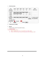
Don’t try to initialize EEPROM, unless software can’t work normally.
2. Alignment procedures:
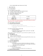
2.1 B+ voltage adjustment
2.1.1
Needn’t adjust B+ voltage on the line.
All relevant connectors and modules must be connected and inserted.
Mains voltage is at 230VAC, 50Hz or 110VAC, 60Hz.
Apply Color Bar Testing Pattern to RF in put.
Adjust VR800 in STANDARD mode
Note:
☆
We recommend this B+ voltage, but each factory PE must adjust many parameters to match the
new tube, and the exact B+ voltage must according to that.
2.1.1
Needn’t adjust B+ voltage on the line.
2.2 Crystal oscillator frequency adjustment
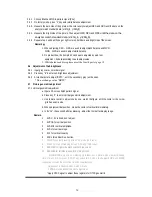
2.2.1 Crystal oscillator frequency adjustment with NICAM
a. Apply PAL BG NICAM signal with good reception quality.
b. Enter factory mode, press “game” key , then press “V+” key to adjust “DCXO Auto”, until it
displays “OKEY”.
2.2.2
Crystal oscillator frequency adjustment without NICAM
a. Input PAL color bar signal.
b. Auto adjustment: Enter factory mode, press “game” key , then press “V+” key to adjust
“DCXO Auto”, until it displays “OKEY”
.
Manual adjustment :On factory mode, press “0” to adjust “DCXO CAP” until DISC steady at 128.
2.3 RF AGC adjustment
2.3.1 Input 58dB grey scale signal.
2.3.2 Press key “4” to enter RF AGC adjustment.
2.3.3 Press “OK”or “EXIT” key to auto adjust RF AGC, also can adjust “RF AGC” by “”volume -/+” key
until the
letter change from “INACTIVE” to ”ACTIVE”.
*
The others use default value.
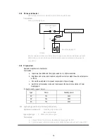
2.4 Screen & Focus voltage adjustment
2.4.1 Screen voltage adjustment
a. Press “MUTE” key on the remote control and the screen will become a horizontal line,
here vertical stop vibration. Then adjust the “screen” VR on the flyback until the horizontal
line can just be seen (minimum visible intensity).
2.4.2 Focus voltage adjustment
a. Input cross hatch pattern signal.
b. Adjust the “focus” VR on the flyback until the screen becomes clear.
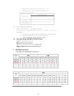
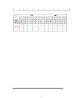
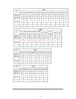
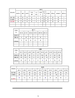
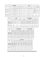
2.5 White balance adjustment (NORMAL)
CRT type
(Part Number)
B+ Voltage
A68ELW021
×
001 140
±
0.3V
A68ELW021
×
003 140
±
0.3V
11
Summary of Contents for SC-29FAS
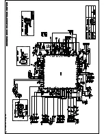
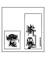
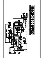
Page 22: ...5 Schematic Diagram ...
Page 23: ......
Page 24: ...24 ...
Page 25: ......
Page 26: ......
Page 29: ...7 PCB Layout ...
Page 30: ......
Page 31: ...31 8 Explode View Diagram ...


