1 INTRODUCTION
RT2048
1.4.
PRINCIPLE OF OPERATION
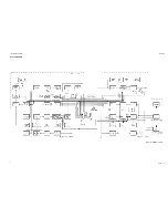
FREQUENCY GENERATION
All the internal frequencies are referenced to a crystal oscillator, running on 14.85 MHz.
The 14.85 MHz is divided by 4 in the REFERENCE DIVIDER, to generate a 3.7125 MHz signal, which is the input
to the PLL-reference divider and clock-signal for the microcomputer.
The local oscillator signal for the first mixer in the receiver and the transmit signal are generated in a phase-locked
loop (PLL). To generate the needed frequencies, which are specified as follows:
139.1 MHZ < fLO1 < 148.45 MHz; 154.5 MHz < fTX NORMAL < 159.15 MHz
159.0 MHz < fTX SPECIAL << 163.75 MHz
a bandshift is performed in the VCO.
The loop reference frequency - and so the resolution - is 12.5 kHz, derived by dividing the reference divider output
with 297.
The VCO output frequency is divided down to 12.5 kHz after the dual-modulus principle with a PRESCALER dividing
with 32/33.
The phase detector output controls the CHARGE PUMPE feeding the loop filter integrator.
If there is a difference in phase/frequency between the inputs to the phase detector. An error current from the charge
pumpe will be integrated in the loop filter, producing the needed voltage for the VCO.
RECEIVER
The antenna signal is fed to the RX AMPLIFIER through the RX/TX relay.
The bandpass filters around the RX amplifier are tuned by means of capacitor diodes, which are controlled by a DC-
voltage derived from the VCO control voltage in the PLL.
The received signal is converted to the first intermediate frequency on 15.3 MHz in the FIRST MIXER, using the VCO
signal from the RX BUFFER AMPLIFIER as local oscillator signal.
The signal is filtered and amplified before down-conversion to 450 kHz in the SECOND MIXER. The crystal oscillator
signal is used as local oscillator signal.
After filtering in the SECOND IF FILTER, the signal is amplified and detected.
The AF signal is passed through a mute switch before undergoing appropriate amplification and filtering to get the
right frequency response.
Besides, the detected output is filtered in the SQUELCH FILTER before it is amplified, detected, and compared with
a reference level to get a logical level for the microcomputer, which controls the mute circuit.
The telephone amplifier and the AF power amplifier produce the wanted output levels for the earpiece and the
loudspeaker.
TRANSMITTER
The signal from the microphone is passed through a PRE-EMPHASIS network before appropriate amplification and
compression in the AF AMPLIFIER COMPRESSOR.
This signal is filtered before it is fed to the VCO, where the modulation of the transmitter signal takes place.
As the VCO oscillates direct on the transmitting frequency in TX-mode, the signal only has to be amplified. This is
done in the TX BUFFER AMPLIFIER and the TX POWER AMPLIFIER.
The power supply for the TX power amplifier is regulated by a feed-back loop via the POWER SENSE circuit to
maintain constant output power level. Switching between full and reduced output power level is made by means of
the PA-REGULATOR.
To reduce the level of harmonic components in the output signal it is passed through a HARMONIC FILTER before
it is led to the antenna via the RX-TX-RELAY.
MICROCOMPUTER
The microcomputer on the interface unit is taking care of various functions, among these the user interface, which
means reading of the keyboard and readout to the LED-display via the DISPLAY-LATCHES.
Moreover the computer calculates the appropriate division figures for the PLL, controls the transmitter power level,
the AF mute circuits, and reads and writes to the EEPROM’s.
When a selcall unit is installed, the microcomputer also controls the selcall switch capacitor filter.
The serial interface is only for factory production use.
9403
Page 1-6
Summary of Contents for RT2048 VHF
Page 1: ...INSTALLATION MANUAL SAILOR RT2048 VHF ...
Page 4: ......
Page 11: ...1 INTRODUCTION RT2048 Page 1 7 9403 BLOCK DIAGRAM ...
Page 12: ......
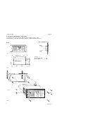
Page 22: ...2 INSTALLATION RT2048 Page 2 10 9346 626945 625473 ...
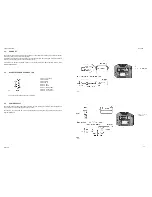
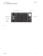
Page 24: ...2 INSTALLATION RT2048 2 8 REAR VIEW OF VHF RT2048 25567 9350 Page 2 11 ...
Page 26: ......
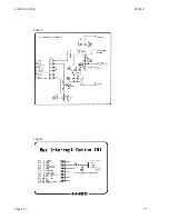
Page 31: ...3 Service RT2048 3 10 PIN CONFIGURATIONS Page 3 5 ...
Page 32: ...3 SERVICE RT2048 Page 3 6 ...
Page 33: ...3 Service RT2048 Page 3 7 ...
Page 34: ...3 SERVICE RT2048 Page 3 8 ...
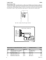
Page 38: ...5 CIRCUIT DESCRIPTION AND SCHEMATIC DIAGRAMS RT2048 Page 5 2 ...
Page 89: ......
Page 90: ...Thrane Thrane A S info thrane com www thrane com M2048GB Issue E 0820 ...


