NXP Semiconductors
UM11637
FRDMGD3160DCMHB evaluation board
6.4 Troubleshooting
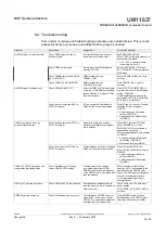
Some common issues and troubleshooting procedures are detailed below. This is not an
exhaustive list by any means, and additional debug may be needed:
Problem
Evaluation
Explanation
Corrective action(s)
Check PWM jumper position on
translator board
Incorrect PWM jumpers obstruct
signal path but not report fault
Set PWMH_SEL (J4) and
PWML_SEL (J5) jumpers properly, for
desired control method:
•
3.3 V to 5.0 V translator board
Check PWM control signal
Ensure that proper PWM signal is
reaching GD3160
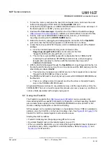
Monitor EXT_PWML (TP14) and
EXT_PWMH (TP15) for commanded
PWM state
Check FSENB status (see GD3160
pin 15, STATUS3)
PWM is disabled when
FSENB = LOW
Set pin FSENB = HIGH (pin 15) to
continue
No PWM output (no fault reported)
Check CONFIG_EN bit (MODE2)
PWM is disabled when
CONFIG_EN is logic 1
Write CONFIG_EN = logic 0 to
continue
Check VGE fault (VGE_FLT)
A short on IGBT or SiC module gate,
or too low of VGEMON delay setting
causes VGE fault, locking out PWM
control of the gate.
Clear VGE_FLT bit (STATUS2) to
continue. Increase VGEMON delay
setting (CONFIG6).
If safe operating condition can be
guaranteed, set VGE_FLTM (MSK2)
bit to logic 0, to mask fault.
No PWM output (fault reported)
Check for short-circuit fault (SC) in
STATUS1 register
SC is a severe fault that disables
PWM. SC fault cannot be masked
Clear SC fault to continue. Consider
adjusting SC fault settings on
GD3160:
•
Adjust short-circuit threshold
setting (CONFIG2)
•
Adjust short-circuit filter setting
(CONFIG2)
Check for dead time fault (DTFLT) in
STATUS2 register
Dead time is enforced, but fault
indicates that PWM controls signals
are in violation
Clear DTFLT fault bit (STATUS2).
Check PWMHSEL (J11) and
PWMLSEL (J10) are configured to
bypass dead time faults.
Consider adjusting dead time settings
on GD3160:
•
Change mandatory PWM dead
time setting (CONFIG5)
•
Mask dead time fault (MSK2)
PWM output is good, but with
persistent fault reported
Check for overcurrent (OC) fault in
STATUS1 register
OC fault latches, but does not disable
PWM. OC fault cannot be masked.
Clear OC fault bit (STATUS1).
Adjust OC fault detection settings on
GD3160:
•
Adjust overcurrent threshold
setting (CONFIG1)
•
Adjust overcurrent filter setting
(CONFIG1)
PWM or FSSTATE rising edge has
longer delay than falling edge
Check translator output voltage
versus GD3160 VDD voltage
Low translator output voltage
(compared with correct VDD at
GD3160) causes the high threshold
at the GD3160 pin to be crossed later
than commanded
Check translator output voltage
selection (J233) is configured to the
same level as the GD3160 VDD
Check VCCSEL supply or translator
outputs on the translator board
for excessive loading or supply
droop/pulldown
WDOG_FLT reported on startup
Check VSUP and VCC are powered
On initialization, watchdog fault is
reported when one die is powered up
before the other
Check VSUP and VCC both have
power applied.
Clear WDOG_FLT bit (STATUS2) to
continue.
SPIERR reported on startup
Check KL25Z/translator connection
On initialization, SPIERR can occur
when the SPI bus is open, or when
GD3160 IC is powered up before the
translator (which provides CSB).
Clear SPIERR fault to continue.
Reinitialize power to GD3160 after
translator is powered (over USB).
UM11637
All information provided in this document is subject to legal disclaimers.
© NXP B.V. 2022. All rights reserved.
User guide
Rev. 2 — 3 February 2022
38 / 42

