


R8C/18 Group, R8C/19 Group
Rev.1.30
Apr 14, 2006
Page 121 of 233
REJ09B0222-0130
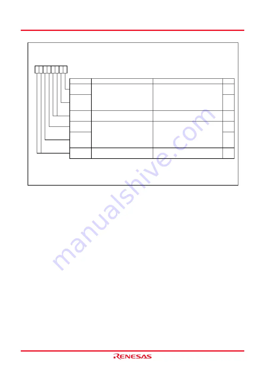
Figure 14.15
TCSS Register
Timer Count Source Setting Register
Symbol
Address
After Reset
TCSS
008Eh
00h
Bit Symbol
Bit Name
Function
RW
NOTE:
1.
—
(b7-b6)
Timer X count source select bits
(1)
Do not sw itch count sources during a count operation. Stop the timer count before sw itching count sources.
RW
Timer Z count source select bits
(1)
b5 b4
0 0 : f1
0 1 : f8
1 0 : Selects Timer X underflow .
1 1 : f2
RW
RW
TZCK1
RW
RW
b7 b6 b5 b4
0 0
b3 b2 b1 b0
RW
—
(b3-b2)
Reserved bits
Set to 0.
Reserved bits
Set to 0.
0
b1 b0
0 0 : f1
0 1 : f8
1 0 : fRING
1 1 : f2
TXCK0
0
TXCK1
TZCK0


